
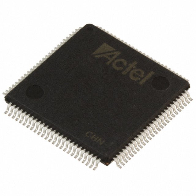
A54SX32A-1TQ100
| Part Description |
SX-A Field Programmable Gate Array (FPGA) IC 81 100-LQFP |
|---|---|
| Quantity | 951 Available (as of June 18, 2026) |

| Product Category | Field Programmable Gate Array (FPGA) |
|---|---|
| Manufacturer | Microchip Technology |
| Manufacturing Status | Obsolete |
| Manufacturer Standard Lead Time | Contact Us |
| Datasheet |
Specifications & Environmental
| Device Package | 100-TQFP (14x14) | Grade | Commercial | Operating Temperature | 0°C – 70°C | ||
|---|---|---|---|---|---|---|---|
| Package / Case | 100-LQFP | Number of I/O | 81 | Voltage | 2.25 V - 5.25 V | ||
| Mounting Method | Surface Mount | RoHS Compliance | RoHS non-compliant | REACH Compliance | REACH Unaffected | ||
| Moisture Sensitivity Level | 3 (168 Hours) | Number of LABs/CLBs | 2880 | Number of Logic Elements/Cells | 2880 | ||
| Number of Gates | 48000 | ECCN | 3A991D | HTS Code | 8542.39.0001 | ||
| Qualification | N/A |
Overview of A54SX32A-1TQ100 – SX-A Field Programmable Gate Array (FPGA) IC 81 100-LQFP
The A54SX32A-1TQ100 is a commercial-grade, nonvolatile SX-A family FPGA offered in a 100-pin LQFP package. It provides a mid-range logic capacity with 48,000 system gates and 2,880 logic elements tailored for board-level digital logic, interface bridging, and glue‑logic functions in commercial embedded systems.
Designed for mixed-voltage systems, the device supports flexible I/O configurations and in-system diagnostics, delivering deterministic timing and board-level integration where a compact, reprogrammable, single-chip solution is required.
Key Features
- Logic Capacity — 48,000 system gates and approximately 2,880 logic elements provide mid-range programmable logic resource for control, glue logic, and interface functions.
- I/O Count & Configurability — 81 user I/O pins in the 100-LQFP package with configurable I/O support for 3.3 V / 5 V PCI, 5 V TTL, 3.3 V LVTTL and 2.5 V LVCMOS2 standards.
- Mixed-Voltage Operation — Supports 2.5 V, 3.3 V, and 5 V mixed-voltage operation with 5 V input tolerance and 5 V drive strength; supply range 2.25 V to 5.25 V.
- Performance — Series-level performance guidance includes up to 250 MHz system performance and up to 350 MHz internal performance for timing‑sensitive logic.
- Power-Up/Down Friendly — Power sequencing is not required for supply voltages, simplifying system power management.
- Hot-Swap Compliant I/Os — I/O behavior supports hot-swap use cases and board-level maintenance scenarios.
- PCI Support — 66 MHz PCI-compliant signaling capability for PCI-based designs and add-on cards.
- System Reliability & Test — Boundary-scan testing (IEEE 1149.1 JTAG) and deterministic, user-controllable timing simplify validation and manufacturing test.
- Security & In-System Diagnostics — Actel Secure Programming Technology (FuseLock™) protects design IP; in-system diagnostic and verification capability is supported via Silicon Explorer II.
- Package & Environmental — Supplied in a 100-LQFP (14×14) package; commercial temperature range 0 °C to 70 °C; RoHS compliant.
Typical Applications
- PCI-based systems — Implement bus interface logic, bridging, or add-in card functions using the device's 66 MHz PCI compliance and configurable I/Os.
- Mixed-voltage system glue logic — Level translation, protocol interfacing, and board glue where 2.5 V / 3.3 V / 5 V I/O compatibility is required.
- Commercial embedded control — Board-level control, peripheral management, and interface aggregation in commercial embedded products operating within 0 °C to 70 °C.
- Manufacturing test & verification — Boundary-scan and in-system diagnostic support for streamlined validation and production testing.
Unique Advantages
- Mid-range, predictable logic resource: 48,000 system gates and ~2,880 logic elements balance integration and cost for commercial designs.
- Flexible I/O for mixed systems: Configurable I/O standards and 5 V tolerance reduce the need for external level-shifters and simplify board design.
- Nonvolatile single-chip solution: Eliminates external configuration memory and simplifies system boot and firmware workflows.
- Design security and testability: FuseLock secure programming plus IEEE 1149.1 boundary-scan and in-system diagnostics improve IP protection and manufacturing efficiency.
- Power and serviceability: Power-up/down friendly operation and hot-swap capable I/Os support robust system maintenance and power sequencing flexibility.
- Compact packaging: 100-LQFP footprint (14×14) enables dense board placement for space-constrained commercial applications.
Why Choose A54SX32A-1TQ100?
The A54SX32A-1TQ100 positions itself as a practical, commercial-grade FPGA choice for designers who need deterministic timing, flexible mixed-voltage I/O, and secure in-system programmability in a compact 100‑pin package. Its mid-range logic capacity and PCI support make it suitable for board-level interface tasks and control logic where a nonvolatile, single-chip FPGA simplifies system architecture.
For teams focused on reliability, testability, and IP protection, this device offers boundary-scan, in-system diagnostics, and FuseLock security, providing long-term value through simplified validation and maintainable hardware designs.
Request a quote or submit a sourcing inquiry to check availability and pricing for the A54SX32A-1TQ100.


Date Founded: 1989
Headquarters: Chandler, Arizona, USA
Employees: 22,000+
Revenue: $8.349 Billion
Certifications and Memberships: ISO9001:2015, IATF16949:2016, AS 9100D


