
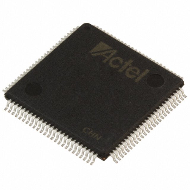
A54SX32A-1TQ100I
| Part Description |
SX-A Field Programmable Gate Array (FPGA) IC 81 100-LQFP |
|---|---|
| Quantity | 325 Available (as of June 15, 2026) |
| Product Category | Field Programmable Gate Array (FPGA) |
|---|---|
| Manufacturer | Microchip Technology |
| Manufacturing Status | Obsolete |
| Manufacturer Standard Lead Time | Contact Us |
| Datasheet |
Specifications & Environmental
| Device Package | 100-TQFP (14x14) | Grade | Industrial | Operating Temperature | -40°C – 85°C | ||
|---|---|---|---|---|---|---|---|
| Package / Case | 100-LQFP | Number of I/O | 81 | Voltage | 2.25 V - 5.25 V | ||
| Mounting Method | Surface Mount | RoHS Compliance | RoHS non-compliant | REACH Compliance | REACH Unaffected | ||
| Moisture Sensitivity Level | 3 (168 Hours) | Number of LABs/CLBs | 2880 | Number of Logic Elements/Cells | 2880 | ||
| Number of Gates | 48000 | ECCN | 3A991D | HTS Code | 8542.39.0001 | ||
| Qualification | N/A |
Overview of A54SX32A-1TQ100I – SX-A Field Programmable Gate Array (FPGA) IC 81 100-LQFP
The A54SX32A-1TQ100I is a nonvolatile SX-A family FPGA from Microchip Technology designed for industrial-temperature embedded logic. It provides 48,000 system gates realized as approximately 2,880 logic elements and up to 81 user I/Os in a 100-pin thin quad flat package.
Built for mixed-voltage systems and deterministic timing applications, the device supports a wide supply range and a suite of configurable I/O options while delivering series-level performance characteristics such as 250 MHz system performance and 350 MHz internal performance.
Key Features
- Core Performance Approximately 48,000 system gates implemented as 2,880 logic elements, delivering the SX-A family’s quoted 250 MHz system and 350 MHz internal performance targets.
- I/O Flexibility Up to 81 user I/Os with configurable support for 3.3 V / 5 V PCI, 5 V TTL, 3.3 V LVTTL and 2.5 V LVCMOS2 signaling; 5 V input tolerance and 5 V drive strength are supported at the series level.
- Nonvolatile Single-Chip SX-A family single-chip, nonvolatile architecture enables in-system configuration without external configuration memory.
- Power and Voltage Wide supply range (2.25 V to 5.25 V) and power-up/power-down friendly operation that requires no supply sequencing.
- System Reliability & Test Boundary-scan testing compliant with IEEE 1149.1 (JTAG) and in-system diagnostic/verification capability provided at the series level.
- Security and Programmability Series-level secure programming technology (FuseLock™) to protect bitstream IP and prevent reverse engineering.
- Signal Control Configurable weak pull-up/pull-down on I/O at power-up and individual output slew-rate control for signal integrity tuning.
- Package & Environmental 100-LQFP package (supplier device package listed as 100-TQFP, 14×14); surface-mount mounting; industrial operating temperature range −40 °C to 85 °C; RoHS compliant.
- Resource Utilization & Timing Series-level support for up to 100% resource utilization and 100% pin locking with deterministic, user-controllable timing.
Typical Applications
- PCI-based systems 66 MHz PCI compliance at the series level supports integration into PCI and legacy bus applications that require programmable logic.
- Industrial embedded control Industrial temperature rating (−40 °C to 85 °C) and robust I/O options suit embedded controllers and automation modules.
- Mixed-voltage interface designs Wide supply range and multi-voltage I/O support enable bridging and interfacing between 5 V and lower-voltage domains.
- Secure in-system programmable logic Nonvolatile, single-chip configuration combined with series-level secure programming enables field-updatable designs with protection against reverse engineering.
Unique Advantages
- Nonvolatile single-chip architecture: Eliminates the need for external configuration memory while enabling in-system programming and instant configuration on power-up.
- Wide supply and mixed-voltage I/O: 2.25 V to 5.25 V supply range plus multi-voltage I/O support allows flexible integration into diverse system power domains.
- Industrial temperature support: Specified for −40 °C to 85 °C operation for deployments in industrial environments.
- Deterministic timing control: Series-level deterministic, user-controllable timing supports designs that require predictable timing closure.
- Security features: FuseLock™ secure programming technology reduces the risk of reverse engineering and protects intellectual property.
- Comprehensive testability: Boundary-scan (IEEE 1149.1) and in-system diagnostic capabilities improve manufacturing test coverage and field diagnostics.
Why Choose A54SX32A-1TQ100I?
The A54SX32A-1TQ100I delivers a compact, nonvolatile FPGA solution with industry-grade operating range, flexible mixed-voltage I/O and a balance of logic capacity (approximately 2,880 logic elements / 48,000 system gates) and I/O density (81 pins) in a 100-pin package. It is positioned for embedded designs that require deterministic timing, secure in-system programmability and compatibility with legacy voltage domains.
Designed as part of the SX-A family from Microchip Technology, this device provides a secure, testable and flexible platform for industrial and mixed-voltage applications where nonvolatile configuration, I/O flexibility and predictable performance are required.
If you would like pricing, availability, or to request a quote for the A54SX32A-1TQ100I, submit an inquiry or request a formal quote today.


Date Founded: 1989
Headquarters: Chandler, Arizona, USA
Employees: 22,000+
Revenue: $8.349 Billion
Certifications and Memberships: ISO9001:2015, IATF16949:2016, AS 9100D


