
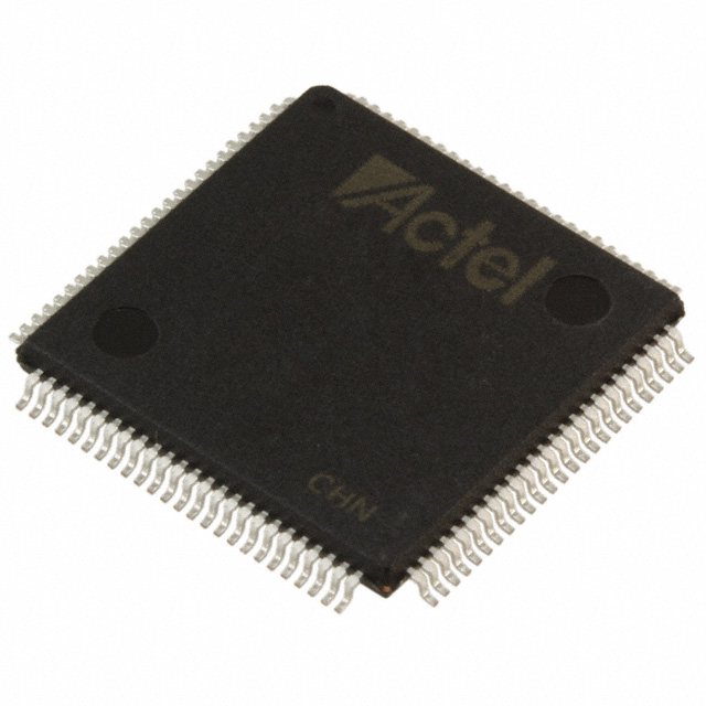
A54SX32A-1TQ144I
| Part Description |
SX-A Field Programmable Gate Array (FPGA) IC 113 144-LQFP |
|---|---|
| Quantity | 1,036 Available (as of June 15, 2026) |

| Product Category | Field Programmable Gate Array (FPGA) |
|---|---|
| Manufacturer | Microchip Technology |
| Manufacturing Status | Obsolete |
| Manufacturer Standard Lead Time | Contact Us |
| Datasheet |
Specifications & Environmental
| Device Package | 144-TQFP (20x20) | Grade | Industrial | Operating Temperature | -40°C – 85°C | ||
|---|---|---|---|---|---|---|---|
| Package / Case | 144-LQFP | Number of I/O | 113 | Voltage | 2.25 V - 5.25 V | ||
| Mounting Method | Surface Mount | RoHS Compliance | RoHS non-compliant | REACH Compliance | REACH Unaffected | ||
| Moisture Sensitivity Level | 3 (168 Hours) | Number of LABs/CLBs | 2880 | Number of Logic Elements/Cells | 2880 | ||
| Number of Gates | 48000 | ECCN | 3A991D | HTS Code | 8542.39.0001 | ||
| Qualification | N/A |
Overview of A54SX32A-1TQ144I – SX-A Field Programmable Gate Array (FPGA) IC 113 144-LQFP
The A54SX32A-1TQ144I is an SX-A family FPGA from Microchip Technology offering a nonvolatile, single‑chip programmable logic solution in a 144‑pin LQFP package. With 48,000 system gates and 2,880 logic elements, this industrial‑grade device targets applications that require flexible, deterministic digital logic in harsh temperature environments.
Built for mixed‑voltage I/O and in‑system programmability, the device supports a broad supply range and features designed for reliable power sequencing, security and boundary‑scan testing, making it suitable for embedded control, interface and I/O customization tasks.
Key Features
- Logic Capacity — 48,000 system gates and 2,880 logic elements provide significant programmable logic density for glue logic, protocol bridging and custom datapath implementations.
- I/O and Voltage Flexibility — 113 user I/Os with configurable I/O support for multiple signaling environments; devices in the SX‑A family support 2.5 V, 3.3 V and 5 V mixed‑voltage operation, with 5 V input tolerance and drive strength options.
- Performance — SX‑A family performance targets include 250 MHz system performance and up to 350 MHz internal performance (family specification); the part number includes a –1 speed grade for increased performance relative to standard speed.
- Package and Mounting — Delivered in a 144‑LQFP surface‑mount package (supplier package: 144‑TQFP, 20×20 mm) suitable for compact board designs.
- Industrial Temperature Grade — Rated for operation from –40 °C to +85 °C, supporting industrial applications and environments.
- Nonvolatile Single‑Chip Configuration — Single‑chip, nonvolatile configuration simplifies system design by eliminating external configuration memory and providing power‑up/power‑down friendly behavior without supply sequencing.
- Security and Test — Includes Actel Secure Programming Technology with FuseLock™ to protect design IP and supports IEEE 1149.1 boundary‑scan (JTAG) for manufacturing test and in‑system diagnostics.
- System Diagnostics and Tool Support — Family‑level support for in‑system diagnostic and verification via Silicon Explorer II (as specified for the SX‑A family).
- Regulatory — RoHS compliant.
Typical Applications
- Industrial control and automation — Implement custom control logic, signal conditioning interfaces and state machines that require industrial temperature operation and flexible I/O.
- Embedded system glue logic — Replace discrete glue components with compact, reprogrammable logic for protocol conversion, bus interfacing and timing control.
- PCI and legacy interface bridging — SX‑A family devices include PCI compliance (66 MHz) and configurable I/O support for 3.3 V/5 V PCI signaling, enabling interface bridging and expansion tasks.
- Communications and instrumentation — Use the device for protocol handling, parallel/serial interface adaptation and deterministic timing functions within measurement and communications equipment.
Unique Advantages
- Single‑chip nonvolatile configuration: Eliminates the need for external configuration memory, simplifying BOM and board layout.
- Flexible mixed‑voltage I/O: Supports multiple I/O voltage standards and 5 V input tolerance for broad compatibility with legacy and modern interfaces.
- Industrial temperature rating: Rated –40 °C to +85 °C to meet the demands of industrial application environments.
- Security features: FuseLock™ secure programming protects intellectual property and helps prevent reverse engineering.
- In‑system diagnostics and testability: Boundary‑scan (IEEE 1149.1) and family‑level diagnostic tools support manufacturing test and in‑field verification.
- Compact package: 144‑LQFP surface‑mount package offers a balance of pin count and board area for space‑constrained designs.
Why Choose A54SX32A-1TQ144I?
The A54SX32A-1TQ144I delivers a practical combination of programmable logic capacity, mixed‑voltage I/O flexibility and industrial temperature operation in a single, nonvolatile device. Its 48,000 system gates and 2,880 logic elements make it well suited for custom control, interface and bridging roles where deterministic timing, in‑system programmability and security are important.
This device is a strong fit for design teams looking to reduce BOM complexity and add field‑reprogrammable capability while maintaining robust testability and IP protection. With RoHS compliance and a compact 144‑pin LQFP package, it supports predictable integration into industrial and embedded products.
Request a quote or contact sales to discuss availability, pricing and how the A54SX32A-1TQ144I can fit into your next design.


Date Founded: 1989
Headquarters: Chandler, Arizona, USA
Employees: 22,000+
Revenue: $8.349 Billion
Certifications and Memberships: ISO9001:2015, IATF16949:2016, AS 9100D


