
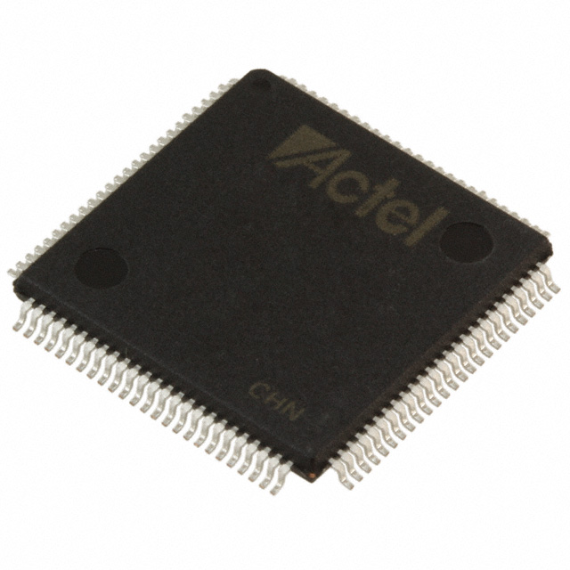
A54SX32A-1TQG100I
| Part Description |
SX-A Field Programmable Gate Array (FPGA) IC 81 100-LQFP |
|---|---|
| Quantity | 443 Available (as of June 15, 2026) |
| Product Category | Field Programmable Gate Array (FPGA) |
|---|---|
| Manufacturer | Microchip Technology |
| Manufacturing Status | Active |
| Manufacturer Standard Lead Time | 12 Weeks |
| Datasheet |
Specifications & Environmental
| Device Package | 100-TQFP (14x14) | Grade | Industrial | Operating Temperature | -40°C – 85°C | ||
|---|---|---|---|---|---|---|---|
| Package / Case | 100-LQFP | Number of I/O | 81 | Voltage | 2.25 V - 5.25 V | ||
| Mounting Method | Surface Mount | RoHS Compliance | ROHS3 Compliant | REACH Compliance | REACH Unaffected | ||
| Moisture Sensitivity Level | 3 (168 Hours) | Number of LABs/CLBs | 2880 | Number of Logic Elements/Cells | 2880 | ||
| Number of Gates | 48000 | ECCN | 3A991D | HTS Code | 8542.39.0001 | ||
| Qualification | N/A |
Overview of A54SX32A-1TQG100I – SX-A Field Programmable Gate Array (FPGA), 81 I/O, 100‑LQFP
The A54SX32A-1TQG100I is an industrial-grade SX-A family FPGA in a 100‑pin LQFP package, offering a nonvolatile, single‑chip programmable logic solution. With 2,880 logic elements (approximately 48,000 system gates) and 81 user I/Os, it targets embedded control, I/O bridging and industrial applications that require configurable logic, mixed‑voltage I/O support and robust operating range.
Built for systems that need deterministic timing and flexible I/O, the device combines series-level performance characteristics (up to 250 MHz system performance and up to 350 MHz internal performance as documented for the SX‑A family) with configuration and security features intended for production embedded designs.
Key Features
- Core Logic 2,880 logic elements providing roughly 48,000 system gates for mid‑range FPGA integration and custom glue‑logic implementation.
- I/O Resources 81 user-configurable I/Os with support for mixed-voltage operation. I/O capabilities in the SX‑A family include 5 V input tolerance and configurable I/O standards.
- Nonvolatile Single‑Chip Configuration SX‑A family devices are provided as a nonvolatile, single‑chip solution for instant-on operation without external configuration memory.
- Performance Series-level documented system performance up to 250 MHz and internal timing up to 350 MHz, enabling responsive control and data-path implementation.
- Power and Voltage Wide supply range from 2.25 V to 5.25 V to support a variety of system rails and mixed-voltage designs.
- Package and Mounting 100‑pin LQFP package (supplier device package: 100‑TQFP, 14×14) in a surface-mount form factor suitable for compact PCB layouts.
- Industrial Temperature Grade Rated for operation from –40°C to 85°C for reliable performance in industrial environments.
- Design and Test Support Series features include boundary‑scan testing (IEEE 1149.1/JTAG) and in‑system diagnostic capabilities for verification and production test.
- Security and IP Protection SX‑A family devices include secure programming technology and device-level protections to protect design IP.
- Regulatory RoHS‑compliant construction to meet environmental requirements for lead‑free assemblies.
Typical Applications
- Industrial Automation — Implement motor control logic, sensor interfacing and deterministic I/O aggregation within industrial control systems using the device’s temperature rating and mixed‑voltage I/O support.
- Embedded Control and Glue Logic — Replace discrete logic with configurable, reprogrammable logic for board-level protocol bridging, timing adaptation and custom control functions.
- Communications and Networking — Use for protocol bridging, data routing or timing-critical logic blocks where series-level MHz performance and configurable I/O are required.
- Instrumentation and Test Equipment — Implement measurement front‑ends, data capture logic and deterministic processing paths leveraging the nonvolatile configuration and boundary‑scan testability.
Unique Advantages
- Flexible I/O Voltage Range: Supports mixed‑voltage operation and a wide supply range (2.25 V to 5.25 V), simplifying integration with legacy 5 V and modern 3.3 V/2.5 V systems.
- Nonvolatile, Single‑Chip Deployment: Eliminates external configuration memory for simpler BOM and reliable instant‑on behavior in embedded products.
- Industrial Reliability: Industrial temperature rating (–40°C to 85°C) and surface‑mount 100‑pin package suitable for rugged production applications.
- Onboard Test and Security: Boundary‑scan (JTAG) and secure programming features facilitate production test and IP protection during deployment.
- Deterministic Timing Capability: Series-level documented internal and system performance enable predictable timing paths for control and data processing tasks.
Why Choose A54SX32A-1TQG100I?
The A54SX32A-1TQG100I positions itself as a reliable mid‑range FPGA choice for industrial and embedded designs that need a nonvolatile, reprogrammable logic device with flexible I/O and a wide supply voltage window. Its combination of approximately 2,880 logic elements, 81 user I/Os, industrial temperature rating and package options makes it suitable for replacing discrete logic, implementing custom protocols, or consolidating glue logic to reduce BOM complexity.
Choose this device when you need a field‑programmable, single‑chip solution that supports mixed‑voltage systems, offers on‑board testability and provides series-level performance characteristics for responsive embedded control and interface tasks.
Request a quote or submit an inquiry to receive pricing and availability information for the A54SX32A-1TQG100I and to discuss how it fits your project requirements.


Date Founded: 1989
Headquarters: Chandler, Arizona, USA
Employees: 22,000+
Revenue: $8.349 Billion
Certifications and Memberships: ISO9001:2015, IATF16949:2016, AS 9100D


