
A54SX32A-1TQG144M
| Part Description |
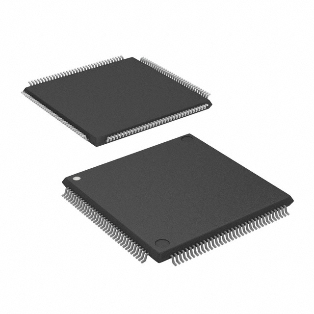
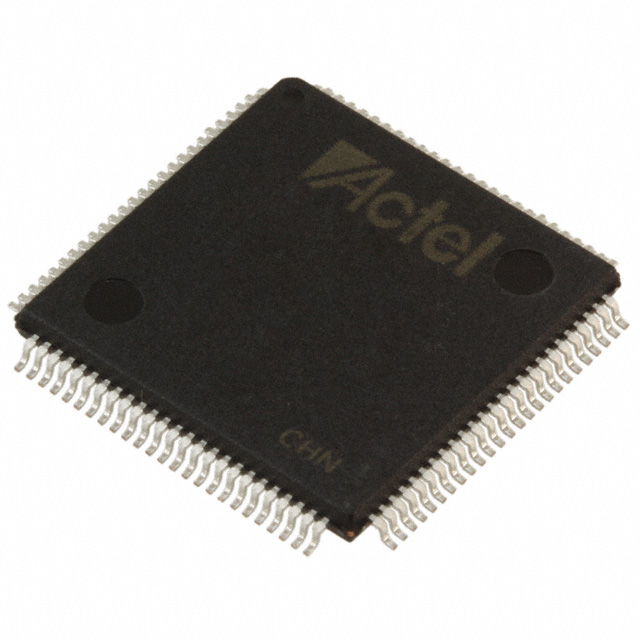
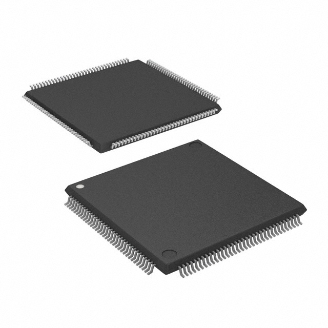
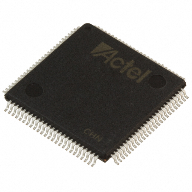
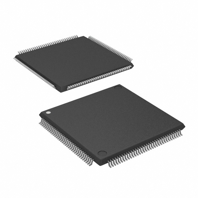
SX-A Field Programmable Gate Array (FPGA) IC 113 144-LQFP |
|---|---|
| Quantity | 654 Available (as of October 8, 2026) |
| Product Category | Field Programmable Gate Array (FPGA) |
|---|---|
| Manufacturer | Microchip Technology |
| Manufacturing Status | Active |
| Manufacturer Standard Lead Time | 20 Weeks |
| Datasheet |
Specifications & Environmental
| Device Package | 144-TQFP (20x20) | Grade | Military | Operating Temperature | -55°C – 125°C | ||
|---|---|---|---|---|---|---|---|
| Package / Case | 144-LQFP | Number of I/O | 113 | Voltage | 2.25 V - 5.25 V | ||
| Mounting Method | Surface Mount | RoHS Compliance | ROHS3 Compliant | REACH Compliance | REACH Unaffected | ||
| Moisture Sensitivity Level | 3 (168 Hours) | Number of LABs/CLBs | 2880 | Number of Logic Elements/Cells | 2880 | ||
| Number of Gates | 48000 | ECCN | 3A001A2C | HTS Code | 8542.39.0001 | ||
| Qualification | N/A |
Overview of A54SX32A-1TQG144M – SX-A Field Programmable Gate Array (FPGA) IC 113 144-LQFP
The A54SX32A-1TQG144M is a military-grade SX-A family field programmable gate array from Microchip Technology. It provides a nonvolatile, single-chip FPGA architecture with 2,880 logic elements and 48,000 system gates, delivering deterministic timing and flexible I/O for high-reliability embedded designs.
Designed for applications that demand wide operating temperature range and robust I/O support, this device targets military and other high-reliability markets where temperature tolerance, configurable I/O voltages and in-system testability are required.
Key Features
- Logic Capacity – Approximately 48,000 system gates implemented across 2,880 logic elements for medium-complexity FPGA functions.
- I/O Count & Flexibility – 113 user-programmable I/O pins with configurable I/O support for 3.3 V / 5 V PCI, 5 V TTL, 3.3 V LVTTL and 2.5 V LVCMOS2 signaling.
- Performance – SX-A family performance characteristics include up to 250 MHz system performance and up to 350 MHz internal performance (family-level data).
- Voltage & Power – Wide supply range of 2.25 V to 5.25 V and support for mixed 2.5 V, 3.3 V and 5 V operation with 5 V input tolerance and 5 V drive strength.
- Package & Mounting – 144-pin LQFP package (supplier device package: 144-TQFP, 20×20) in a surface-mount form factor suitable for high-reliability assemblies.
- Temperature & Grade – Military grade device with operating temperature range from −55 °C to +125 °C.
- Memory – On-chip RAM: 0 total RAM bits; combinational and sequential logic realized using logic elements (2,880) and dedicated flip-flops per device architecture.
- Nonvolatile Single-Chip – Family-level single-chip nonvolatile configuration eliminates the need for separate configuration memory.
- I/O & System Features – Hot-swap compliant I/Os, power-up/power-down friendly operation (no supply sequencing required), selectable weak pull-up or pull-down on I/O at power-up, and individual output slew rate control (family-level).
- Test & Security – Boundary-scan (IEEE 1149.1/JTAG) support and Actel Secure Programming technology with FuseLock™ for protection against reverse engineering (family-level).
Typical Applications
- Military & Aerospace Systems – Leverage military-grade temperature range and wide-voltage support for control, data routing and interface consolidation in rugged environments.
- High-Reliability Embedded Control – Implement deterministic logic and timing for mission-critical control, signal processing and embedded sequencing.
- PCI and Bus Interface Design – Support for 66 MHz PCI signaling and multiple I/O voltage standards enables protocol bridging and legacy bus interfacing.
- In-System Diagnostics & Verification – Use built-in boundary-scan and family-level in-system diagnostic capabilities for board-level test and verification workflows.
Unique Advantages
- Wide Operating Range: Military-grade temperature rating (−55 °C to +125 °C) ensures suitability for extreme-environment deployments.
- Flexible Voltage Interfacing: Broad supply range (2.25 V–5.25 V) and configurable I/O levels simplify mixed-voltage system integration.
- Nonvolatile, Single-Chip Configuration: Eliminates external configuration memory and simplifies system boot and field updates.
- Robust I/O Feature Set: Hot-swap compliance, power-up friendly behavior and selectable pull options reduce board-level sequencing and interface complexity.
- Security & Testability: Boundary-scan and FuseLock™ secure programming provide design protection and support for production test flows.
Why Choose A54SX32A-1TQG144M?
The A54SX32A-1TQG144M combines the SX-A family’s nonvolatile FPGA architecture with a military temperature grade and broad I/O flexibility to address medium-complexity, high-reliability applications. Its 2,880 logic elements and approximately 48,000 system gates deliver the capacity needed for control, interfacing and deterministic logic functions while removing the need for external configuration storage.
This device is well suited for engineers and procurement teams developing systems that require wide temperature operation, mixed-voltage I/O support and in-system testability. The family-level performance characteristics and integrated security/test features provide a clear upgrade path for designs that must balance integration, reliability and field programmability.
Request a quote or submit an inquiry to get pricing and availability for the A54SX32A-1TQG144M. Our team can provide lead-time details and ordering information for your design requirements.





















Date Founded: 1989
Headquarters: Chandler, Arizona, USA
Employees: 22,000+
Revenue: $8.349 Billion
Certifications and Memberships: ISO9001:2015, IATF16949:2016, AS 9100D




