
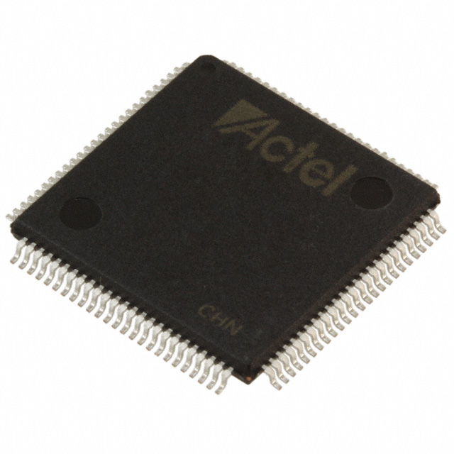
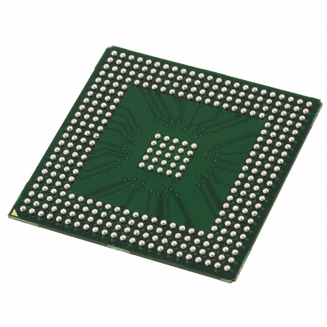
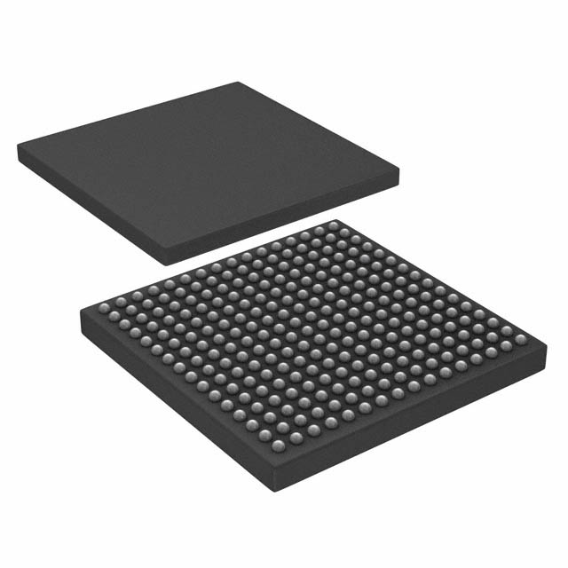
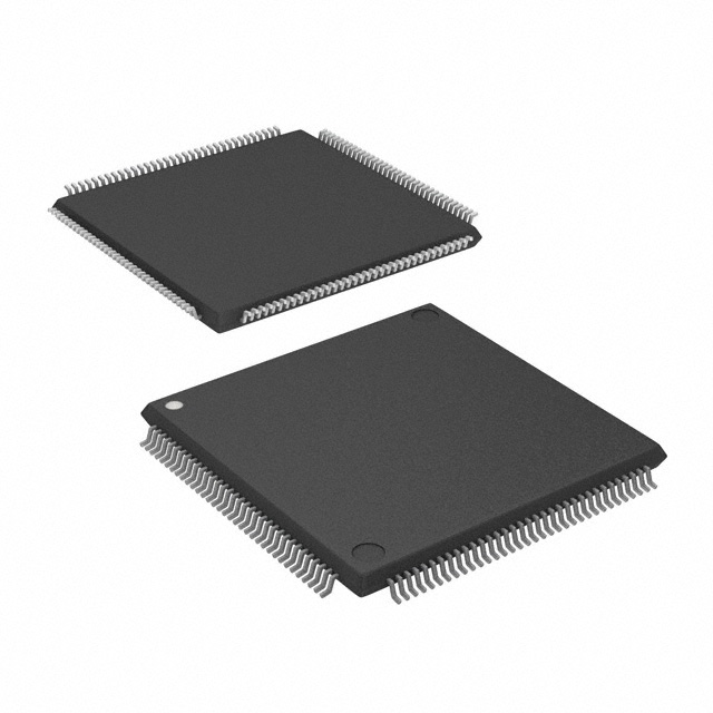
A54SX32A-2BG329
| Part Description |
SX-A Field Programmable Gate Array (FPGA) IC 249 329-BBGA |
|---|---|
| Quantity | 1,395 Available (as of June 18, 2026) |

| Product Category | Field Programmable Gate Array (FPGA) |
|---|---|
| Manufacturer | Microchip Technology |
| Manufacturing Status | Active |
| Manufacturer Standard Lead Time | 20 Weeks |
| Datasheet |
Specifications & Environmental
| Device Package | 329-PBGA (31x31) | Grade | Commercial | Operating Temperature | 0°C – 70°C | ||
|---|---|---|---|---|---|---|---|
| Package / Case | 329-BBGA | Number of I/O | 249 | Voltage | 2.25 V - 5.25 V | ||
| Mounting Method | Surface Mount | RoHS Compliance | RoHS non-compliant | REACH Compliance | REACH Unaffected | ||
| Moisture Sensitivity Level | 3 (168 Hours) | Number of LABs/CLBs | 2880 | Number of Logic Elements/Cells | 2880 | ||
| Number of Gates | 48000 | ECCN | 3A991D | HTS Code | 8542.39.0001 | ||
| Qualification | N/A |
Overview of A54SX32A-2BG329 – SX-A Field Programmable Gate Array (FPGA) IC 249 329-BBGA
The A54SX32A-2BG329 is a commercial-grade FPGA from Microchip Technology’s SX-A family. It provides a nonvolatile, single-chip FPGA architecture with 48,000 system gates, approximately 2,880 logic elements and up to 249 user I/Os in a 329-ball BGA package.
Designed for system designs that require mixed-voltage I/O, in-system configuration and PCI-compatible interfaces, this device combines high I/O density, configurable I/O standards and on-chip security features to simplify board-level integration and IP protection.
Key Features
- Core & Capacity – Approximately 48,000 system gates and 2,880 logic elements provide a mid-range FPGA resource set for glue-logic, protocol bridging and control plane functions.
- I/O & Interface Flexibility – Up to 249 user-programmable I/Os with configurable support for 3.3 V / 5 V PCI, 5 V TTL, 3.3 V LVTTL and 2.5 V LVCMOS2 to accommodate mixed-voltage systems and legacy interfaces.
- Performance – SX-A family performance characteristics include system-level operation to 250 MHz and internal performance to 350 MHz, with this part using the –2 speed grade (approximately 25% faster than standard).
- Power & Voltage – Wide voltage supply support from 2.25 V to 5.25 V and mixed-voltage operation on I/Os enable flexible power architectures without complex sequencing.
- Security & Test – Nonvolatile single-chip configuration with Actel Secure Programming Technology (FuseLock™) to help protect design IP, plus boundary-scan (IEEE 1149.1) for board-level testability.
- System Reliability – Hot-swap compliant I/Os and power-up/power-down friendly operation reduce system-level power sequencing constraints and support robust board behavior during field events.
- Package & Grade – Supplied in a 329-ball PBGA (31 × 31 mm) package; commercial temperature grade (0 °C to +70 °C). RoHS compliant.
- On-chip Resources – This device reports zero on-chip RAM bits (Total RAM Bits: 0), making it suitable for logic-centric implementations where external memory is preferred.
Typical Applications
- PCI and legacy bus interfaces – Use the device’s 66 MHz PCI compliance and configurable 3.3 V / 5 V I/O support to implement host/bus interface logic and bridge functions.
- Mixed-voltage system glue – High I/O count and mixed-voltage I/O capability make the part well suited for interfacing between 5 V legacy devices and lower-voltage cores.
- Secure configuration and IP protection – Leverage the nonvolatile configuration and FuseLock programming to protect critical firmware and reduce the risk of reverse engineering.
- Hot-swap and field-serviceable boards – Hot-swap compliant I/Os and power-up/power-down friendly behavior enable use on boards that require live insertion/removal or tolerant power sequencing.
Unique Advantages
- High I/O density: Up to 249 user I/Os allow complex board-level interconnects and multiple peripheral interfaces without external multiplexing.
- Mixed-voltage support: Configurable I/O standards and 2.25 V–5.25 V supply range simplify integration with diverse voltage domains.
- Nonvolatile, single-chip solution: Eliminates the need for external configuration memory and supports deterministic power-up behavior.
- Security-focused programming: FuseLock technology helps protect design IP and deter reverse engineering.
- Board-level testability: IEEE 1149.1 boundary-scan support facilitates production test and in-system diagnostics.
- Commercial-grade thermal profile: Rated for 0 °C to +70 °C for board designs targeting commercial environments.
Why Choose A54SX32A-2BG329?
The A54SX32A-2BG329 delivers a balanced combination of mid-range logic capacity, high I/O count and mixed-voltage flexibility in a nonvolatile FPGA. Its SX-A family attributes—system/internal performance figures, hot-swap I/Os, and in-system security—make it suitable for commercial designs that require stable configuration behavior, IP protection and direct interfacing to legacy and modern I/O standards.
Choose this device when your design demands a commercial-grade, single-chip FPGA solution with 48,000 system gates, approximately 2,880 logic elements and up to 249 user I/Os in a 329-ball PBGA package. The device’s predictable configuration model and test/security features support longer-term maintainability and integration within mixed-voltage systems.
Request a quote or submit an RFQ to obtain pricing and availability for the A54SX32A-2BG329. Our team can provide lead-time details and ordering information to support your design schedule.


Date Founded: 1989
Headquarters: Chandler, Arizona, USA
Employees: 22,000+
Revenue: $8.349 Billion
Certifications and Memberships: ISO9001:2015, IATF16949:2016, AS 9100D


