
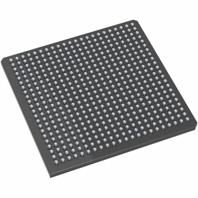
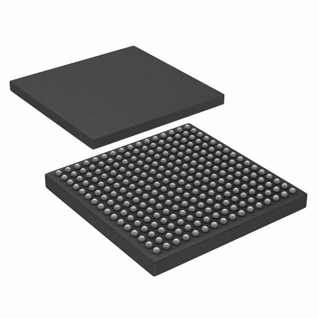
A54SX32A-2FG484
| Part Description |
SX-A Field Programmable Gate Array (FPGA) IC 249 484-BGA |
|---|---|
| Quantity | 1,539 Available (as of June 10, 2026) |

| Product Category | Field Programmable Gate Array (FPGA) |
|---|---|
| Manufacturer | Microchip Technology |
| Manufacturing Status | Active |
| Manufacturer Standard Lead Time | 52 Weeks |
| Datasheet |
Specifications & Environmental
| Device Package | 484-FPBGA (27X27) | Grade | Commercial | Operating Temperature | 0°C – 70°C | ||
|---|---|---|---|---|---|---|---|
| Package / Case | 484-BGA | Number of I/O | 249 | Voltage | 2.25 V - 5.25 V | ||
| Mounting Method | Surface Mount | RoHS Compliance | RoHS non-compliant | REACH Compliance | REACH Unaffected | ||
| Moisture Sensitivity Level | 3 (168 Hours) | Number of LABs/CLBs | 2880 | Number of Logic Elements/Cells | 2880 | ||
| Number of Gates | 48000 | ECCN | 3A991D | HTS Code | 8542.39.0001 | ||
| Qualification | N/A |
Overview of A54SX32A-2FG484 – SX-A Field Programmable Gate Array (FPGA) IC 249 484-BGA
The A54SX32A-2FG484 is a commercial-grade member of the SX-A family of nonvolatile FPGAs. It delivers a mid-range logic capacity with 48,000 system gates and 2,880 logic elements in a 484‑ball fine-pitch BGA package targeted at embedded control, interface, and I/O‑dense applications.
Built for mixed-voltage system environments, the device combines high I/O density (249 user I/Os) with in-system programmability, boundary-scan support and security features to simplify integration and protect designs.
Key Features
- Logic Capacity Approximately 48,000 system gates and 2,880 logic elements for mid-range digital logic integration.
- I/O Density & Flexibility 249 user-programmable I/Os with hot-swap compliant I/Os and configurable pull-up/pull-down at power-up to support complex board-level interfacing.
- Performance SX-A family published performance metrics include up to 250 MHz system performance and up to 350 MHz internal performance (family values).
- Voltage & I/O Standards Supports mixed-voltage operation (2.5 V, 3.3 V, and 5 V) with 5 V input tolerance and 5 V drive strength; datasheet documents configurable I/O for 3.3 V/5 V PCI, 5 V TTL, 3.3 V LVTTL and 2.5 V LVCMOS2.
- Power Supply Device supply range: 2.25 V to 5.25 V to accommodate a variety of system power rails.
- Nonvolatile Single-Chip Architecture SX-A family devices are provided as nonvolatile, single-chip FPGAs—eliminating the need for external configuration memory.
- Security & Test Actel Secure Programming Technology with FuseLock™ for design protection and IEEE 1149.1 boundary-scan (JTAG) for board-level testability.
- Deterministic Timing & Utilization Datasheet documents deterministic, user-controllable timing plus support for up to 100% resource utilization and 100% pin locking.
- Package & Mounting 484‑BGA package (supplier device package: 484‑FPBGA, 27 × 27 mm); surface-mount mounting type.
- Commercial Grade Grade: Commercial with operating temperature range 0 °C to 70 °C and RoHS compliant packaging.
- Embedded Memory Total RAM bits: 0 (no on-chip RAM reported for this device).
Typical Applications
- PCI and Legacy Interface Logic PCI-compliant signaling capability and configurable I/O standards make the device suitable for interface bridging and legacy bus logic.
- Embedded Control & Glue Logic Mid-range gate count and high I/O density support aggregation of control functions and system glue logic into a single nonvolatile device.
- Board-Level Test & Secure Configuration Boundary-scan and FuseLock secure programming simplify manufacturing test and protect intellectual property on deployed boards.
Unique Advantages
- High I/O Count: 249 user I/Os enable dense peripheral and bus connectivity without external I/O expanders.
- Mixed-Voltage Support: Broad mixed-voltage operation and 5 V tolerance simplify interfacing to both legacy 5 V logic and modern 2.5/3.3 V domains.
- Nonvolatile Single-Chip Solution: Removes the need for external configuration memory, reducing BOM and simplifying board design.
- Design Security: FuseLock secure programming technology helps protect against reverse engineering and unauthorized cloning.
- Deterministic Timing: User-controllable timing and support for full resource utilization aid predictable system integration and timing closure.
- Commercial and RoHS Compliant: Commercial grade with RoHS‑compliant packaging for standard commercial product deployments.
Why Choose A54SX32A-2FG484?
The A54SX32A-2FG484 balances mid-level logic capacity (48k system gates, 2,880 logic elements) with high I/O density (249 pins) in a compact 484‑ball FBGA. Its nonvolatile single-chip architecture, mixed-voltage I/O flexibility, and family-level performance figures make it well suited for system designers consolidating interface, control, and glue logic while retaining secure in-field configuration.
For commercial embedded applications that require dense I/O, secure programming, and board-level testability within a 0 °C to 70 °C operating range, this device offers a practical combination of integration, configurability, and ecosystem-level features documented in the SX-A family datasheet.
Request a quote or contact sales to discuss availability, pricing, and delivery for the A54SX32A-2FG484.


Date Founded: 1989
Headquarters: Chandler, Arizona, USA
Employees: 22,000+
Revenue: $8.349 Billion
Certifications and Memberships: ISO9001:2015, IATF16949:2016, AS 9100D


