
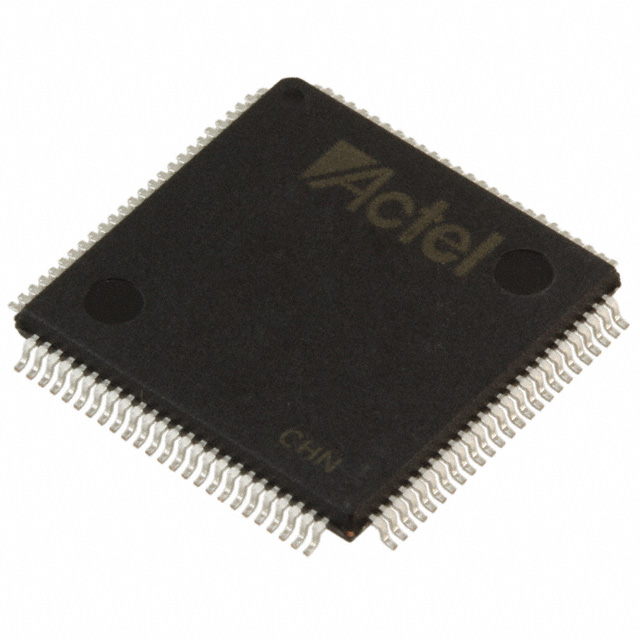
A54SX32A-2PQ208
| Part Description |
SX-A Field Programmable Gate Array (FPGA) IC 174 208-BFQFP |
|---|---|
| Quantity | 740 Available (as of June 15, 2026) |

| Product Category | Field Programmable Gate Array (FPGA) |
|---|---|
| Manufacturer | Microchip Technology |
| Manufacturing Status | Obsolete |
| Manufacturer Standard Lead Time | Contact Us |
| Datasheet |
Specifications & Environmental
| Device Package | 208-PQFP (28x28) | Grade | Commercial | Operating Temperature | 0°C – 70°C | ||
|---|---|---|---|---|---|---|---|
| Package / Case | 208-BFQFP | Number of I/O | 174 | Voltage | 2.25 V - 5.25 V | ||
| Mounting Method | Surface Mount | RoHS Compliance | RoHS non-compliant | REACH Compliance | REACH Unaffected | ||
| Moisture Sensitivity Level | 3 (168 Hours) | Number of LABs/CLBs | 2880 | Number of Logic Elements/Cells | 2880 | ||
| Number of Gates | 48000 | ECCN | 3A991D | HTS Code | 8542.39.0001 | ||
| Qualification | N/A |
Overview of A54SX32A-2PQ208 – SX-A Field Programmable Gate Array (FPGA) IC 174 208-BFQFP
The A54SX32A-2PQ208 is an SX-A family FPGA in a 208-pin PQFP surface-mount package. It provides a nonvolatile, single-chip FPGA architecture with 48,000 system gates and 2,880 logic elements targeted for embedded logic, interface bridging and board-level programmable functions.
Built for mixed-voltage systems, the device supports 2.25 V to 5.25 V supplies, up to 174 user I/Os, and commercial temperature operation (0 °C to +70 °C). The SX-A family offers high internal and system performance characteristics suitable for demanding synchronous designs.
Key Features
- Core Performance SX-A family performance targets include up to 250 MHz system performance and up to 350 MHz internal performance (family specification).
- Logic Capacity Approximately 48,000 system gates and 2,880 logic elements provide substantial programmable logic for mid-density designs.
- I/O Flexibility 174 user I/Os with configurable I/O support for multiple voltage standards; I/Os offer hot-swap compliance and configurable weak pull-up/pull-down at power-up (family features).
- Voltage and Mixed-Voltage Operation Supports 2.25 V to 5.25 V supply range with 5 V input tolerance and 5 V drive strength options (family feature), enabling mixed-voltage board designs.
- Packaging & Mounting 208-pin PQFP (28 × 28 mm) surface-mount package (208-BFQFP / 208-PQFP) suitable for standard PCB assembly processes.
- Commercial Temperature Grade Rated for commercial operation from 0 °C to +70 °C.
- No Embedded RAM Total on-chip RAM bits: 0 — suitable for designs that use external memory or do not require embedded SRAM.
- System-Level Features Nonvolatile single-chip configuration, power-up/down friendly operation (no supply sequencing required), and boundary-scan (JTAG) test support for production and in-system debug (family features).
- Security and Diagnostics Family-level secure programming technology (FuseLock™) to protect designs and in-system diagnostic/verification capability with Silicon Explorer II (family features).
- Standards and Interfaces 66 MHz PCI compliance capability at the family level for designs requiring legacy PCI interfacing.
- RoHS Compliant Device is RoHS compliant for environmental and supply-chain compatibility.
Typical Applications
- PCI Interface and Bridge Logic Implement PCI-compatible interface logic using the family’s 66 MHz PCI compliance and configurable I/O options.
- Board-Level Glue Logic Replace discrete glue logic and CPLDs with a single, reprogrammable device to reduce BOM and simplify board routing.
- Production Test and In-System Diagnostics Use boundary-scan (JTAG) and the family’s in-system diagnostic features to streamline production test and field verification.
- Secure, Programmable Functions Apply FuseLock™ secure programming for applications requiring protection against reverse engineering and unauthorized copying.
Unique Advantages
- Nonvolatile Single-Chip Solution: Eliminates the need for external configuration memory while simplifying board design and boot behavior.
- Wide Voltage Support: 2.25 V to 5.25 V supply range and 5 V I/O tolerance enable flexible integration into mixed-voltage systems.
- High Resource Utilization: Family support for up to 100% resource utilization and 100% pin locking provides predictable placement and routing control.
- Power-Up/Down Friendly: No supply sequencing required, reducing power-rail complexity during system bring-up and shutdown.
- Production Testability: Boundary-scan support and in-system diagnostic capability improve manufacturing yield and reduce debugging time.
- Commercial Temperature Suitability: Designed for standard commercial environments (0 °C to +70 °C), matching typical embedded and consumer applications.
Why Choose A54SX32A-2PQ208?
The A54SX32A-2PQ208 combines a nonvolatile SX-A family FPGA architecture with mid-density logic capacity (48,000 gates, 2,880 logic elements) and flexible I/O for mixed-voltage systems. Its family-level performance characteristics, in-system diagnostics, and secure programming options make it a practical choice for designs that require reprogrammable logic, production testability, and protection of intellectual property.
This device is well suited to customers building embedded platforms, board-level interface logic, and applications that benefit from a single-chip, nonvolatile FPGA in a 208-pin PQFP package. Its RoHS compliance and surface-mount package support standard manufacturing processes while enabling upgradeable and serviceable hardware designs.
Request a quote or submit an RFQ to obtain pricing and availability for the A54SX32A-2PQ208.


Date Founded: 1989
Headquarters: Chandler, Arizona, USA
Employees: 22,000+
Revenue: $8.349 Billion
Certifications and Memberships: ISO9001:2015, IATF16949:2016, AS 9100D


