
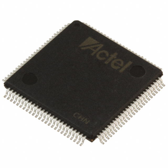
A54SX32A-2PQ208I
| Part Description |
SX-A Field Programmable Gate Array (FPGA) IC 174 208-BFQFP |
|---|---|
| Quantity | 572 Available (as of June 15, 2026) |

| Product Category | Field Programmable Gate Array (FPGA) |
|---|---|
| Manufacturer | Microchip Technology |
| Manufacturing Status | Obsolete |
| Manufacturer Standard Lead Time | Contact Us |
| Datasheet |
Specifications & Environmental
| Device Package | 208-PQFP (28x28) | Grade | Industrial | Operating Temperature | -40°C – 85°C | ||
|---|---|---|---|---|---|---|---|
| Package / Case | 208-BFQFP | Number of I/O | 174 | Voltage | 2.25 V - 5.25 V | ||
| Mounting Method | Surface Mount | RoHS Compliance | RoHS non-compliant | REACH Compliance | REACH Unaffected | ||
| Moisture Sensitivity Level | 3 (168 Hours) | Number of LABs/CLBs | 2880 | Number of Logic Elements/Cells | 2880 | ||
| Number of Gates | 48000 | ECCN | 3A991D | HTS Code | 8542.39.0001 | ||
| Qualification | N/A |
Overview of A54SX32A-2PQ208I – SX-A Field Programmable Gate Array (FPGA) IC 174 208-BFQFP
The A54SX32A-2PQ208I is a nonvolatile SX-A family FPGA offered by Microchip Technology, packaged in a 208-pin BFQFP. It provides a mid-range logic capacity and a rich set of configurable I/O for use in industrial and embedded designs requiring deterministic timing and in-system diagnostics.
Designed for mixed-voltage operation and industrial temperature ranges, this device targets system and peripheral control, embedded processing glue logic, and interfaces where nonvolatile single-chip configurability and robust I/O flexibility are required.
Key Features
- Logic Capacity: Approximately 48,000 system gates implemented as 2,880 logic elements, supporting a range of moderate-complexity logic functions.
- I/O and Package: 174 user-programmable I/O pins in a 208-BFQFP (208-PQFP, 28×28) surface-mount package—suited for dense, board-level implementations.
- Core Performance: SX-A family performance characteristics include up to 250 MHz system performance and up to 350 MHz internal performance (family specification).
- Nonvolatile Single-Chip Configuration: Single-chip, nonvolatile architecture eliminates the need for external configuration memory and supports deterministic, user-controllable timing.
- Mixed-Voltage I/O and Wide VCC Range: Configurable I/O supports multiple voltage standards with a device supply range of 2.25 V to 5.25 V and 5 V input tolerance (family-level capability).
- Industrial Grade and Temperature Range: Rated for industrial operation with an operating temperature range of −40 °C to 85 °C.
- System Reliability and Test: Boundary-scan testing compliant with IEEE 1149.1 (JTAG) and in-system diagnostic/verification capability (Silicon Explorer II) for easier production test and field diagnostics (family features).
- Mounting and Compliance: Surface-mount device with RoHS-compliant status.
Typical Applications
- Industrial Control: Implement motor control logic, timing-critical I/O sequencing, and interface bridging where industrial temperature range and robust I/O are required.
- PCI and Peripheral Interfaces: Use in PCI-compliant peripheral logic and interface adaptation thanks to family-level PCI support and configurable I/O voltage options.
- Embedded System Glue Logic: Replace multiple discrete components with a single nonvolatile FPGA for board-level glue logic and control functions.
- In-System Diagnostics and Test: Leverage boundary-scan and the family’s in-system diagnostic capabilities for manufacturing test, debugging, and field verification.
Unique Advantages
- Nonvolatile Single-Chip Solution: Eliminates external configuration memory and simplifies power-up sequencing for more predictable system behavior.
- Flexible I/O and Voltage Support: Wide supply voltage range and configurable I/O enable mixed-voltage designs and 5 V-tolerant interfaces, reducing the need for level-shifters.
- Deterministic Timing: User-controllable timing and predictable performance characteristics support timing-critical designs.
- Industrial Qualification: Rated for −40 °C to 85 °C operation, making it suitable for industrial environments.
- Production Test and Security: Boundary-scan support and family-level Secure Programming Technology help streamline manufacturing test and protect design IP.
Why Choose A54SX32A-2PQ208I?
The A54SX32A-2PQ208I positions itself as a practical, nonvolatile FPGA choice for designers who need a mid-range logic device with extensive I/O and robust industrial operating conditions. With roughly 48,000 system gates and 2,880 logic elements, plus 174 user I/Os in a 208-pin surface-mount package, it delivers integration and flexibility for embedded control, interface conversion, and production-test-friendly designs.
Backed by Microchip Technology’s SX-A family documentation and features such as deterministic timing, boundary-scan testing, and mixed-voltage I/O support, this device suits teams focused on reliable, maintainable designs that benefit from single-chip configuration and in-system diagnostic capabilities.
Request a quote or submit an inquiry to purchase the A54SX32A-2PQ208I and discuss availability and pricing with our sales team.


Date Founded: 1989
Headquarters: Chandler, Arizona, USA
Employees: 22,000+
Revenue: $8.349 Billion
Certifications and Memberships: ISO9001:2015, IATF16949:2016, AS 9100D


