
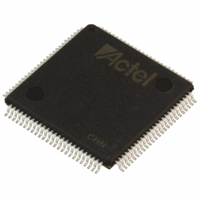
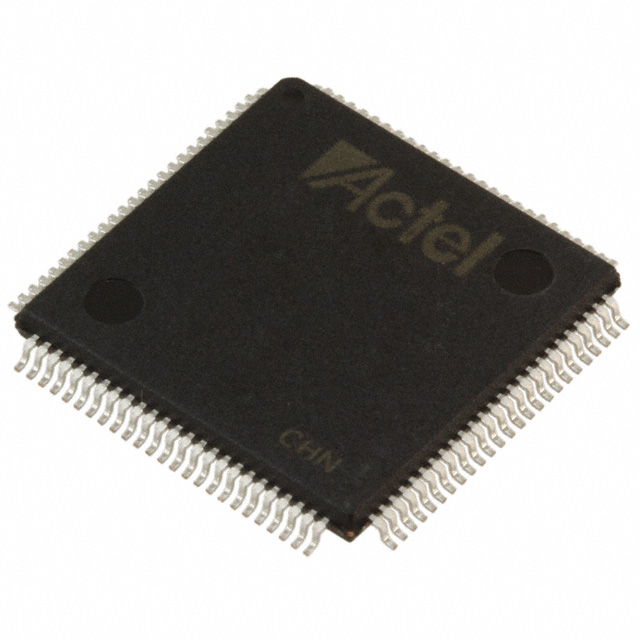
A54SX32A-TQ100A
| Part Description |
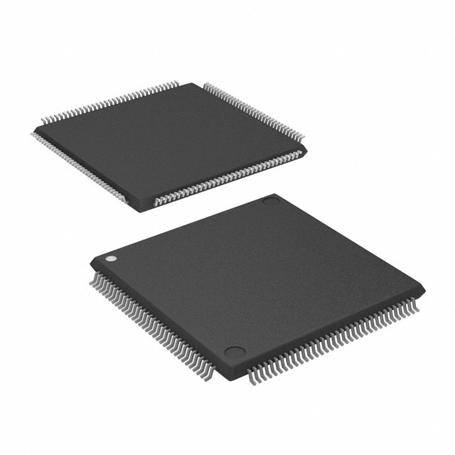
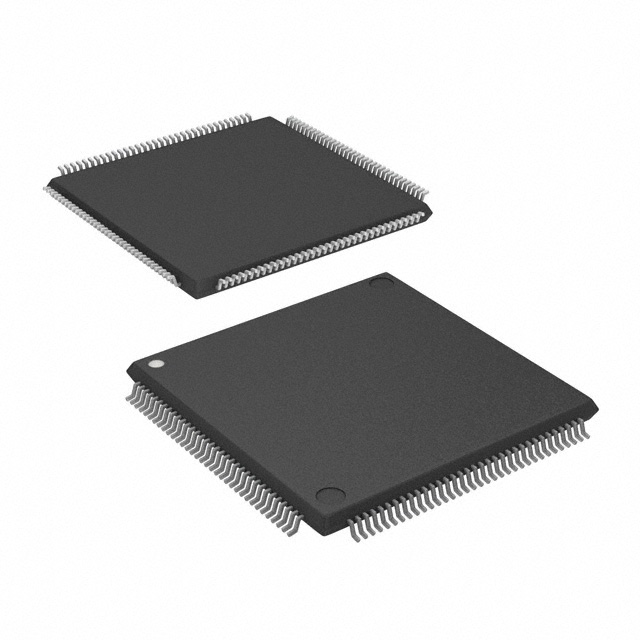
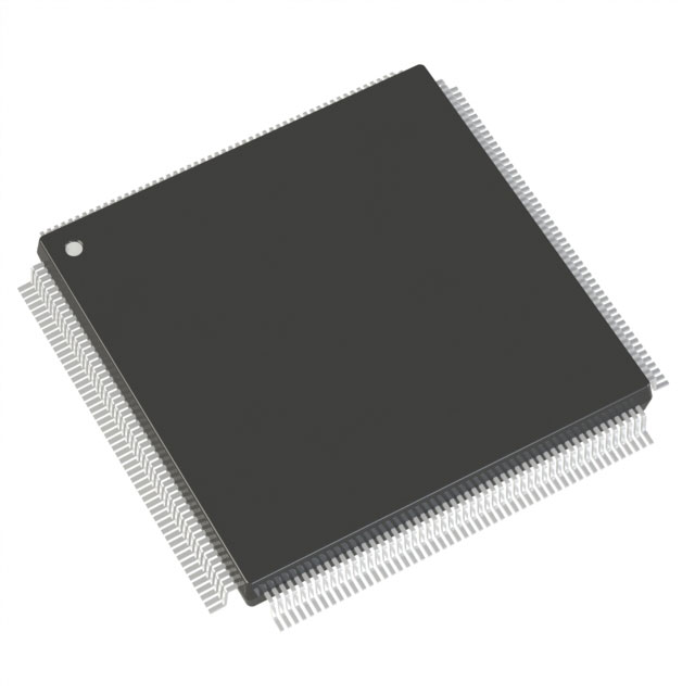
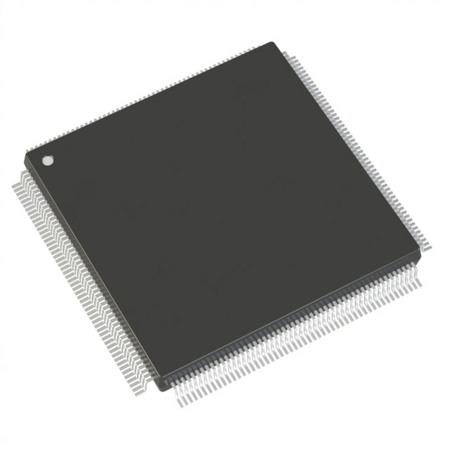
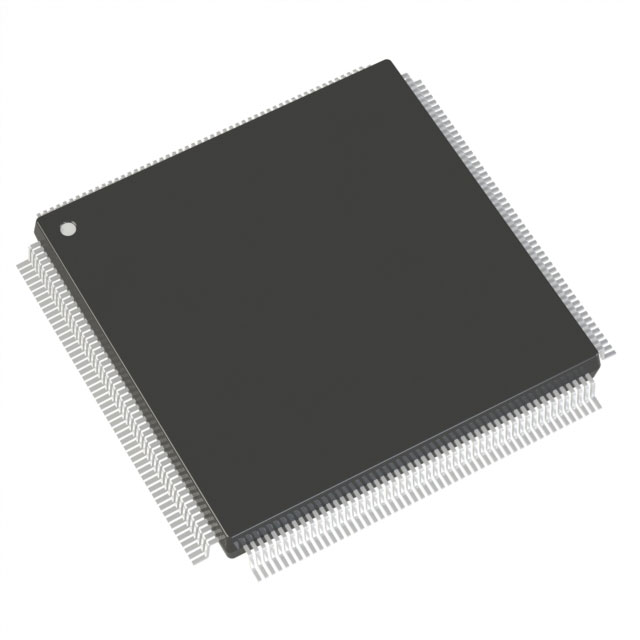
SX-A Field Programmable Gate Array (FPGA) IC 81 100-LQFP |
|---|---|
| Quantity | 367 Available (as of October 8, 2026) |
| Product Category | Field Programmable Gate Array (FPGA) |
|---|---|
| Manufacturer | Microchip Technology |
| Manufacturing Status | Obsolete |
| Manufacturer Standard Lead Time | Contact Us |
| Datasheet |
Specifications & Environmental
| Device Package | 100-TQFP (14x14) | Grade | Automotive | Operating Temperature | -40°C – 125°C | ||
|---|---|---|---|---|---|---|---|
| Package / Case | 100-LQFP | Number of I/O | 81 | Voltage | 2.25 V - 5.25 V | ||
| Mounting Method | Surface Mount | RoHS Compliance | RoHS non-compliant | REACH Compliance | REACH Unaffected | ||
| Moisture Sensitivity Level | 3 (168 Hours) | Number of LABs/CLBs | 2880 | Number of Logic Elements/Cells | 2880 | ||
| Number of Gates | 48000 | ECCN | 3A991D | HTS Code | 8542.39.0001 | ||
| Qualification | AEC-Q100 |
Overview of A54SX32A-TQ100A – SX-A Field Programmable Gate Array (FPGA) IC 81 I/O 100-LQFP
The A54SX32A-TQ100A is an SX-A family field programmable gate array supplied by Microchip Technology. It provides a nonvolatile, single-chip FPGA architecture with approximately 48,000 system gates and 2,880 logic elements, targeted for applications requiring deterministic timing and configurable I/O.
Designed and qualified for automotive use (AEC-Q100), this surface-mount FPGA combines flexible I/O voltage support (2.25 V to 5.25 V), up to 81 user I/Os in a 100-pin TQFP/LQFP package, and an extended operating range of −40 °C to 125 °C to meet demanding embedded application environments.
Key Features
- Core Logic Approximately 2,880 logic elements (combinatorial cells) and a typical capacity of 48,000 gates provide mid-range programmable logic resources suitable for control and interface functions.
- Programmable Registers Dedicated flip-flop resources (as provided in the SX-A family) support synchronous designs and deterministic timing.
- I/O Flexibility Up to 81 user-programmable I/Os on the 100-pin package; configurable I/O support for 3.3 V PCI, 3.3 V LVTTL and 2.5 V LVCMOS2 as defined by the SX-A family.
- Voltage and Power Wide supply voltage range from 2.25 V to 5.25 V enables interfacing with diverse system rails without special sequencing required at power-up or power-down.
- Automotive Qualification Automotive grade with AEC-Q100 qualification and an operating temperature range of −40 °C to 125 °C for demanding vehicle environments.
- Performance & Timing Family-level characteristics include internal performance up to 250 MHz and deterministic, user-controllable timing for predictable system behavior.
- Nonvolatile Configuration Nonvolatile single-chip architecture retains configuration without external configuration memory.
- System Test & Security Family features include boundary-scan (IEEE 1149.1 JTAG) for test and Actel’s Secure Programming Technology (FuseLock™) to protect designs.
- Package & Mounting 100-pin TQFP/LQFP surface-mount package (14×14 mm supplier device package) for compact board integration.
- Standards & Interfaces SX-A family devices provide 66 MHz PCI compliance and hot-swap compliant I/Os as part of the device family feature set.
Typical Applications
- Automotive control modules AEC-Q100 qualification and −40 °C to 125 °C operating range support in-vehicle control and interface logic where robust thermal and electrical behavior is required.
- Sensor and actuator interfaces Configurable I/O levels and wide supply range enable direct interfacing to a variety of sensors and actuators within embedded systems.
- Deterministic timing functions On-chip dedicated registers and family-level deterministic timing suit timing-critical control and signal-processing tasks.
Unique Advantages
- Highly integrated mid-density FPGA: 48,000 system gates and 2,880 logic elements deliver substantial programmable logic in a compact 100-pin package to reduce BOM and board area.
- Automotive-ready qualification: AEC-Q100 rating and extended temperature range position the device for vehicle-grade applications requiring qualification traceability.
- Flexible I/O and supply support: Configurable I/O standards and 2.25 V–5.25 V supply range simplify integration with mixed-voltage systems.
- Nonvolatile, single-chip configuration: Eliminates the need for external configuration memory and simplifies system boot behavior.
- Built-in testability and security: Boundary-scan (JTAG) support and FuseLock™ secure programming help protect IP and enable in-system diagnostics.
- Predictable performance: Family-level internal performance characteristics and user-controllable timing support reliable, deterministic designs.
Why Choose A54SX32A-TQ100A?
The A54SX32A-TQ100A is positioned as a mid-density, automotive-grade FPGA that balances programmable logic capacity, configurable I/O flexibility, and nonvolatile operation in a compact 100-pin surface-mount package. Its AEC-Q100 qualification, wide supply range, and extended temperature rating make it appropriate for embedded systems requiring durable, predictable behavior under automotive environmental conditions.
This device suits design teams building control, interface, and timing-deterministic subsystems that benefit from on-chip security, boundary-scan testability, and single-chip nonvolatile configuration—delivering long-term robustness and streamlined integration with varied system voltages.
Request a quote or submit an inquiry to obtain pricing and availability for the A54SX32A-TQ100A.





















Date Founded: 1989
Headquarters: Chandler, Arizona, USA
Employees: 22,000+
Revenue: $8.349 Billion
Certifications and Memberships: ISO9001:2015, IATF16949:2016, AS 9100D




