
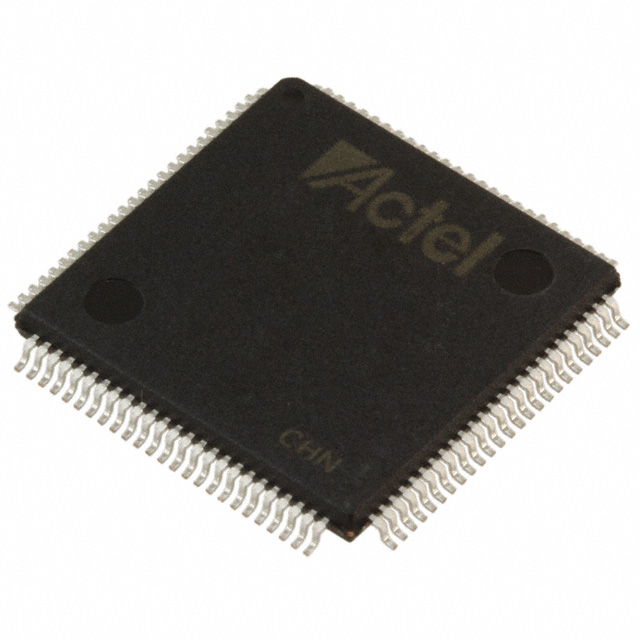
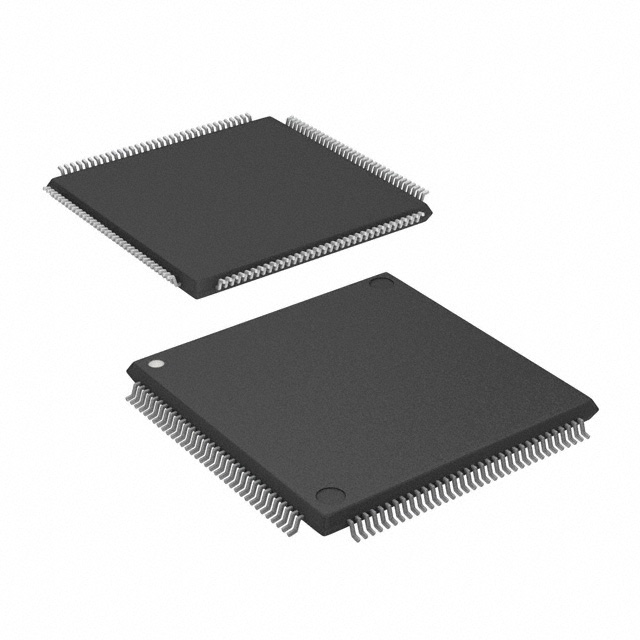
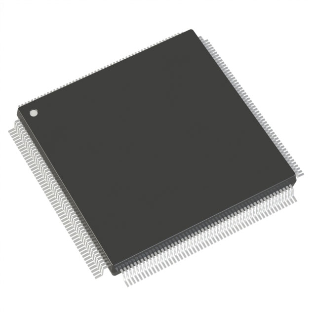
A54SX32A-TQ144
| Part Description |
SX-A Field Programmable Gate Array (FPGA) IC 113 144-LQFP |
|---|---|
| Quantity | 1,754 Available (as of June 15, 2026) |

| Product Category | Field Programmable Gate Array (FPGA) |
|---|---|
| Manufacturer | Microchip Technology |
| Manufacturing Status | Obsolete |
| Manufacturer Standard Lead Time | Contact Us |
| Datasheet |
Specifications & Environmental
| Device Package | 144-TQFP (20x20) | Grade | Commercial | Operating Temperature | 0°C – 70°C | ||
|---|---|---|---|---|---|---|---|
| Package / Case | 144-LQFP | Number of I/O | 113 | Voltage | 2.25 V - 5.25 V | ||
| Mounting Method | Surface Mount | RoHS Compliance | RoHS non-compliant | REACH Compliance | REACH Unaffected | ||
| Moisture Sensitivity Level | 3 (168 Hours) | Number of LABs/CLBs | 2880 | Number of Logic Elements/Cells | 2880 | ||
| Number of Gates | 48000 | ECCN | 3A991D | HTS Code | 8542.39.0001 | ||
| Qualification | N/A |
Overview of A54SX32A-TQ144 – SX-A Field Programmable Gate Array (FPGA) IC 113 144-LQFP
The A54SX32A-TQ144 is a commercial-grade FPGA from Microchip Technology’s SX‑A family. It provides a nonvolatile, single-chip FPGA architecture with 48,000 system gates and approximately 2,880 logic elements, designed for mixed-voltage systems and general-purpose embedded applications.
With 113 user I/Os in the 144-pin LQFP package and a wide supply range (2.25 V to 5.25 V), this device targets applications that require configurable I/O levels, in-system programmability and boundary-scan support at commercial temperature ranges (0 °C to 70 °C).
Key Features
- Logic Capacity 48,000 system gates and approximately 2,880 logic elements (cells) for implementing medium-complexity logic and glue‑logic functions.
- User I/O 113 user-configurable I/O pins in the 144-pin package to support multiple external interfaces and board-level connectivity.
- Nonvolatile Single-Chip Architecture SX‑A family nonvolatile configuration provides single-chip operation without external configuration memory.
- Mixed-Voltage I/O Support Series-level support for 2.5 V, 3.3 V and 5 V mixed-voltage operation with 5 V input tolerance and configurable I/O standards (as provided in SX‑A family documentation).
- Power and Supply Operates from 2.25 V to 5.25 V, allowing flexibility for different board power domains.
- Package and Mounting Surface-mount 144-LQFP package (supplier device package also listed as 144-TQFP, 20×20) for compact PCB designs.
- Commercial Temperature Grade Rated for 0 °C to 70 °C operation for commercial applications.
- Development and Test Support SX‑A family features include JTAG boundary-scan testing and in-system diagnostic/verification capability (per family documentation).
- Security Family-level secure programming technology (FuseLock™) to help protect design IP against reverse engineering (as documented for SX‑A devices).
- Compliance RoHS compliant.
Typical Applications
- PCI and Bus Interface Logic Suitable for implementing PCI-compliant interface logic and board-level bus glue since the SX‑A family documentation lists 66 MHz PCI compliance.
- Mixed-Voltage Interface Bridging Use the device where multiple I/O voltage domains and 5 V-tolerant inputs are needed for level translation or legacy interface support.
- In-System Programmable Logic Ideal for applications that benefit from nonvolatile, single-chip FPGAs with in-system diagnostics and JTAG boundary-scan for production test and field verification.
Unique Advantages
- Nonvolatile, single-chip solution: Eliminates the need for external configuration memory, simplifying BOM and startup behavior.
- Flexible I/O and voltage tolerance: Broad supply range and family-level mixed-voltage I/O support enable interfacing with 2.5 V, 3.3 V and 5 V systems.
- Significant logic density for mid-range designs: 48,000 system gates and ~2,880 logic elements provide ample resources for glue logic, protocol handling, and custom I/O functions.
- Production and field testability: JTAG boundary-scan and in-system diagnostic capabilities (documented for the SX‑A family) support manufacturing test and in-field troubleshooting.
- Secure programming option: Family-level FuseLock™ technology helps protect intellectual property and design confidentiality.
- Compact, surface-mount package: 144-pin LQFP offers a balance of I/O count and PCB footprint suitable for space-constrained designs.
Why Choose A54SX32A-TQ144?
The A54SX32A-TQ144 positions itself as a reliable, mid-density, nonvolatile FPGA option for commercial embedded designs that require mixed-voltage interfacing, in-system programmability and on-board testability. Its combination of 48,000 system gates, roughly 2,880 logic elements and 113 user I/Os in a 144-pin surface-mount package delivers a practical balance of capacity and board-level integration.
This device is well suited for designers seeking an FPGA with single-chip nonvolatile configuration, boundary-scan test support and flexible I/O voltage options within a commercial temperature range. RoHS compliance and broad supply voltage acceptance further simplify adoption across a variety of PCB power architectures.
Request a quote or submit an inquiry to get pricing, availability and additional ordering information for the A54SX32A-TQ144.


Date Founded: 1989
Headquarters: Chandler, Arizona, USA
Employees: 22,000+
Revenue: $8.349 Billion
Certifications and Memberships: ISO9001:2015, IATF16949:2016, AS 9100D


