
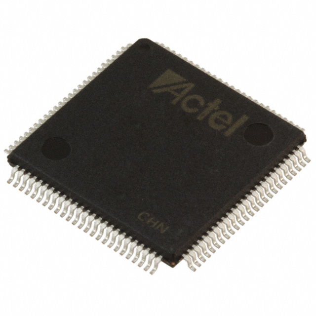
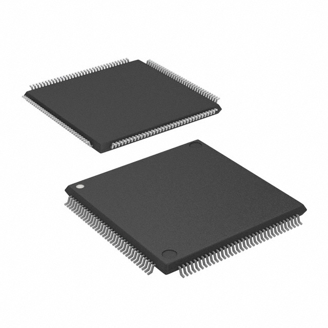
A54SX32A-TQ100M
| Part Description |
SX-A Field Programmable Gate Array (FPGA) IC 81 100-LQFP |
|---|---|
| Quantity | 1,208 Available (as of June 15, 2026) |
| Product Category | Field Programmable Gate Array (FPGA) |
|---|---|
| Manufacturer | Microchip Technology |
| Manufacturing Status | Obsolete |
| Manufacturer Standard Lead Time | Contact Us |
| Datasheet |
Specifications & Environmental
| Device Package | 100-TQFP (14x14) | Grade | Military | Operating Temperature | -55°C – 125°C | ||
|---|---|---|---|---|---|---|---|
| Package / Case | 100-LQFP | Number of I/O | 81 | Voltage | 2.25 V - 5.25 V | ||
| Mounting Method | Surface Mount | RoHS Compliance | RoHS non-compliant | REACH Compliance | REACH Unaffected | ||
| Moisture Sensitivity Level | 3 (168 Hours) | Number of LABs/CLBs | 2880 | Number of Logic Elements/Cells | 2880 | ||
| Number of Gates | 48000 | ECCN | 3A001A2C | HTS Code | 8542.39.0001 | ||
| Qualification | N/A |
Overview of A54SX32A-TQ100M – SX-A Field Programmable Gate Array (FPGA) IC 81 100-LQFP
The A54SX32A-TQ100M is a military-grade SX-A family FPGA from Microchip Technology offered in a 100-pin thin LQFP surface-mount package. It provides a nonvolatile single-chip FPGA solution with a balance of logic capacity, configurable I/O and wide operating ranges for designs requiring robust, deterministic programmable logic.
Targeted at applications that require high-reliability operation and mixed-voltage interfacing, the device combines 48,000 system gates and 2,880 logic elements with a broad supply voltage range and extended temperature rating to support demanding embedded systems.
Key Features
- Logic Capacity — 48,000 system gates and approximately 2,880 logic elements provide significant programmable logic resources for mid-density designs.
- I/O and Voltage Flexibility — 81 user I/O pins with configurable I/O support and mixed-voltage operation across 2.25 V to 5.25 V, enabling direct interfacing with a range of peripheral voltage domains.
- Family Performance — SX-A family performance characteristics include up to 250 MHz system performance and up to 350 MHz internal performance for timing-critical logic (SX-A family specification).
- Nonvolatile Single-Chip Architecture — Family-level single-chip, nonvolatile configuration removes the need for external configuration memory and supports power-up/power-down friendly operation without supply sequencing (SX-A family specification).
- Robust I/O Features — Hot-swap compliant I/Os, 5 V input tolerance, configurable weak pull-up/pull-down at power-up, and individual output slew rate control offer flexible signal integrity and board-level design options (SX-A family specification).
- Security and Test — SX-A family devices support Actel Secure Programming technology with FuseLock™ for protection against reverse engineering and include IEEE 1149.1 boundary-scan (JTAG) for interconnect testability and in-system diagnostics.
- Package and Mounting — 100-pin thin LQFP (TQFP 14×14) surface-mount package for compact board placement and standard PCB assembly flows.
- Temperature and Grade — Military-grade device with an operating temperature range of −55 °C to +125 °C for deployment in harsh and mission-critical environments.
- Compliance — RoHS compliant.
Typical Applications
- Military and Defense Electronics — Military-grade temperature rating and rugged packaging make the device suitable for mission-critical control, signal processing, and interface logic in defense systems.
- High-Reliability Embedded Control — Nonvolatile single-chip configuration and JTAG boundary-scan support robust in-system diagnostics and field maintenance for embedded controllers.
- Mixed-Voltage Interface Bridging — Configurable I/O and wide supply range enable protocol bridging and interface logic between 2.5 V, 3.3 V and 5 V domains.
- Deterministic Logic and Timing — Family-level deterministic, user-controllable timing makes the FPGA suitable for designs that require predictable latency and timing closure.
Unique Advantages
- Military-Grade Reliability: Specified for −55 °C to +125 °C operation and offered in a military grade, supporting deployment in harsh environments.
- Nonvolatile, Power-Friendly Design: Single-chip nonvolatile architecture eliminates external configuration memory and supports power-up/power-down without supply sequencing, simplifying system power management.
- Flexible Mixed-Voltage I/O: 81 configurable I/Os with 5 V tolerance and mixed-voltage operation reduce the need for level shifters and simplify board design.
- Security and Testability: FuseLock™ secure programming and IEEE 1149.1 boundary-scan enable protection of intellectual property and enhanced test coverage.
- Strong Performance Envelope: SX-A family performance ratings (up to 250 MHz system, up to 350 MHz internal) suit timing-sensitive logic implementations.
- Compact, Surface-Mount Package: 100-pin thin LQFP package provides a compact footprint for space-constrained PCBs while supporting standard surface-mount assembly.
Why Choose A54SX32A-TQ100M?
The A54SX32A-TQ100M delivers a balance of mid-range logic capacity, flexible mixed-voltage I/O, and military-grade environmental performance. Its nonvolatile, single-chip architecture and family-level features such as deterministic timing, secure programming, and robust I/O functionality make it a pragmatic choice for high-reliability embedded systems and interface logic applications.
Designers looking for a compact, surface-mount FPGA with proven family capabilities and extended temperature performance will find the A54SX32A-TQ100M appropriate for applications that require dependable operation, in-system testability and configurable I/O without external configuration memory.
Request a quote or contact sales to discuss pricing, availability and design support for the A54SX32A-TQ100M.


Date Founded: 1989
Headquarters: Chandler, Arizona, USA
Employees: 22,000+
Revenue: $8.349 Billion
Certifications and Memberships: ISO9001:2015, IATF16949:2016, AS 9100D


