
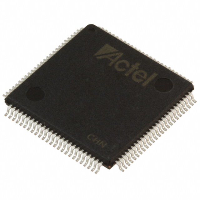
A54SX32A-TQ144M
| Part Description |
SX-A Field Programmable Gate Array (FPGA) IC 113 144-LQFP |
|---|---|
| Quantity | 86 Available (as of June 17, 2026) |

| Product Category | Field Programmable Gate Array (FPGA) |
|---|---|
| Manufacturer | Microchip Technology |
| Manufacturing Status | Obsolete |
| Manufacturer Standard Lead Time | Contact Us |
| Datasheet |
Specifications & Environmental
| Device Package | 144-TQFP (20x20) | Grade | Military | Operating Temperature | -55°C – 125°C | ||
|---|---|---|---|---|---|---|---|
| Package / Case | 144-LQFP | Number of I/O | 113 | Voltage | 2.25 V - 5.25 V | ||
| Mounting Method | Surface Mount | RoHS Compliance | RoHS non-compliant | REACH Compliance | REACH Unaffected | ||
| Moisture Sensitivity Level | 3 (168 Hours) | Number of LABs/CLBs | 2880 | Number of Logic Elements/Cells | 2880 | ||
| Number of Gates | 48000 | ECCN | 3A001A2C | HTS Code | 8542.39.0001 | ||
| Qualification | N/A |
Overview of A54SX32A-TQ144M – SX-A FPGA, 48,000 Gates, 113 I/Os, 144-LQFP
The A54SX32A-TQ144M is a Microchip SX-A family field programmable gate array (FPGA) offered in a 144-pin LQFP/TQFP package and specified for military temperature operation. It delivers a nonvolatile, single‑chip FPGA architecture with 48,000 system gates and 2,880 logic elements suitable for control, I/O bridging and deterministic timing applications.
Designed for systems requiring flexible I/O voltage support and extended temperature range, the device provides hot‑swap–compatible I/Os, mixed‑voltage operation and on‑chip security and test features to support robust embedded designs.
Key Features
- Core Capacity — 48,000 system gates and 2,880 logic elements provide significant programmable logic resources for moderate-complexity designs.
- Performance — System performance up to 250 MHz and internal performance up to 350 MHz as specified for the SX-A family.
- I/O Count & Flexibility — 113 user I/O pins with configurable I/O support for 3.3 V / 5 V PCI, 5 V TTL, 3.3 V LVTTL and 2.5 V LVCMOS2, enabling interface compatibility across voltage domains.
- Mixed‑Voltage Operation — Supports 2.5 V, 3.3 V and 5 V mixed‑voltage operation with 5 V input tolerance and 5 V drive strength; supply range 2.25 V to 5.25 V.
- System Reliability & Test — Hot‑swap compliant I/Os, power‑up/down friendly operation (no sequencing required), and IEEE‑1149.1 boundary‑scan (JTAG) support for board-level testability.
- Security & In-System Diagnostics — Nonvolatile single‑chip configuration with Actel (SX-A) secure programming technology and in‑system diagnostic and verification capability.
- Package & Mounting — Surface mount device in a 144‑pin LQFP/TQFP (20 × 20) package, RoHS compliant and available in military temperature grade (−55 °C to 125 °C).
Typical Applications
- Military and Rugged Electronics — Military temperature rating and robust packaging make the device suited for high‑reliability controllers and interface logic in harsh environments.
- System I/O Bridging — Configurable I/Os and mixed‑voltage support enable level translation, protocol bridging and peripheral interfaces across 2.5 V, 3.3 V and 5 V domains.
- Deterministic Control Logic — High internal performance and deterministic timing capabilities support real‑time control and timing‑sensitive state machines.
- Board‑Level Test and Repair — Boundary‑scan and in‑system diagnostics assist production test, field diagnostics and firmware verification workflows.
Unique Advantages
- Nonvolatile Single‑Chip Solution: Eliminates the need for external configuration memory, simplifying board design and cold-start behavior.
- Wide I/O Voltage Support: Configurable I/Os and mixed‑voltage operation reduce level‑shifter components and lower BOM for multi‑voltage systems.
- Extended Temperature Range: Military grade specification (−55 °C to 125 °C) enables deployment in demanding thermal environments.
- Built‑In Test and Security: Boundary‑scan (IEEE‑1149.1) and secure programming features provide design protection and support manufacturing test flows.
- Deterministic Performance: Documented system and internal performance figures (250 MHz / 350 MHz) help in designing predictable timing paths.
Why Choose A54SX32A-TQ144M?
The A54SX32A-TQ144M combines a substantial logic resource set (48,000 gates, 2,880 logic elements) with flexible, mixed‑voltage I/Os and military temperature qualification to address embedded designs that require durable, deterministic programmable logic. Its nonvolatile single‑chip architecture and onboard test/security capabilities simplify system integration while supporting production test and in‑field verification.
This device is well suited for engineers building control, interface and timing‑sensitive subsystems where I/O flexibility, extended temperature operation and on‑chip programmability reduce BOM and streamline system qualification.
Request a quote or submit an inquiry to learn more about availability, lead times and ordering for A54SX32A-TQ144M.


Date Founded: 1989
Headquarters: Chandler, Arizona, USA
Employees: 22,000+
Revenue: $8.349 Billion
Certifications and Memberships: ISO9001:2015, IATF16949:2016, AS 9100D


