
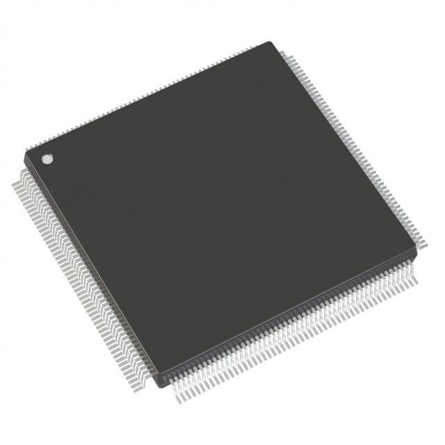
A54SX72A-1PQ208M
| Part Description |
SX-A Field Programmable Gate Array (FPGA) IC 171 208-BFQFP |
|---|---|
| Quantity | 165 Available (as of June 15, 2026) |
| Product Category | Field Programmable Gate Array (FPGA) |
|---|---|
| Manufacturer | Microchip Technology |
| Manufacturing Status | Obsolete |
| Manufacturer Standard Lead Time | Contact Us |
| Datasheet |
Specifications & Environmental
| Device Package | 208-PQFP (28x28) | Grade | Military | Operating Temperature | -55°C – 125°C | ||
|---|---|---|---|---|---|---|---|
| Package / Case | 208-BFQFP | Number of I/O | 171 | Voltage | 2.25 V - 5.25 V | ||
| Mounting Method | Surface Mount | RoHS Compliance | RoHS non-compliant | REACH Compliance | REACH Unaffected | ||
| Moisture Sensitivity Level | 3 (168 Hours) | Number of LABs/CLBs | 6036 | Number of Logic Elements/Cells | 6036 | ||
| Number of Gates | 108000 | ECCN | 3A001A2C | HTS Code | 8542.39.0001 | ||
| Qualification | N/A |
Overview of A54SX72A-1PQ208M – SX-A FPGA, 171 I/O, 208‑BFQFP
The A54SX72A-1PQ208M is a nonvolatile SX-A family Field Programmable Gate Array (FPGA) IC from Microchip Technology, supplied in a 208‑pin BFQFP package. It delivers a high-capacity, deterministic programmable fabric with military-grade temperature capability for designs that require robust operation from −55 °C to +125 °C.
Designed for high-reliability and mission-critical applications, this device combines 108,000 system gates and 6,036 logic elements with 171 user I/Os and flexible mixed-voltage I/O support to simplify interface design and system integration.
Key Features
- Logic Capacity 108,000 system gates and 6,036 logic elements provide substantial programmable logic density for complex control, glue-logic and protocol implementations.
- Dedicated Registers Up to 2,012 dedicated flip‑flops for synchronous logic and state storage.
- I/O Count & Flexibility 171 user-programmable I/Os with configurable I/O support for 5 V TTL, 3.3 V LVTTL, 2.5 V LVCMOS2 and PCI signaling; supports mixed-voltage operation and 5 V input tolerance/drive strength as documented for the SX‑A family.
- Voltage Range Wide device supply range from 2.25 V to 5.25 V to accommodate varied system rail architectures.
- Performance SX‑A family performance metrics include up to 250 MHz system performance and up to 350 MHz internal performance; this part is the –1 speed grade (≈15% faster than standard) per SX‑A datasheet.
- Nonvolatile Single‑Chip Solution Nonvolatile configuration on a single chip simplifies system boot and eliminates external configuration memory.
- Reliability & Test Boundary-scan (IEEE 1149.1) support enables standardized board-level test; devices are power‑up/power‑down friendly and include hot‑swap compliant I/Os.
- Security & Diagnostics Family features include secure programming technology (FuseLock™) and in-system diagnostic/verification capability with Silicon Explorer II as described in the SX‑A documentation.
- Package & Thermal 208‑pin BFQFP (supplier device package 208‑PQFP, 28×28 mm) and military temperature grade operation (−55 °C to +125 °C).
- Embedded Memory No on‑chip RAM bits (Total RAM Bits = 0), useful for designs that rely on external memory or pure logic/flip‑flop based state machines.
Typical Applications
- Military and Aerospace Systems Radiation-tolerant environments are not claimed here, but the device’s military temperature rating and high reliability suit control, interfacing and custom logic tasks in ruggedized equipment.
- Communications & Protocol Bridging Use as programmable glue logic or protocol translators where deterministic timing and a large number of I/Os are required.
- High‑Reliability Control Embedded controllers, sequencers and device supervisors that demand nonvolatile configuration and reliable operation across wide temperature ranges.
- Secure or IP‑Protected Designs Applications requiring on-chip programming security and in-system verification during development and field updates.
Unique Advantages
- High Logic Density: 108,000 system gates and 6,036 logic elements enable consolidation of complex logic into a single device, reducing BOM and board area.
- Mixed‑Voltage I/O Support: Flexible I/O voltage options and 5 V tolerance simplify interfacing to legacy and modern logic families without external translators.
- Nonvolatile, Single‑Chip Configuration: Eliminates external configuration memory and simplifies power-up behavior for secure, reliable system bring-up.
- Military‑Grade Temperature Range: Rated for −55 °C to +125 °C, suitable for thermally demanding environments and long-term fielded systems.
- Deterministic Timing & Testability: Family-level features include deterministic timing control and IEEE 1149.1 boundary-scan for robust design verification and manufacturing test.
- Security & Diagnostics: Built‑in secure programming (FuseLock™) and in‑system diagnostic capabilities support IP protection and easier debug during development.
Why Choose A54SX72A-1PQ208M?
The A54SX72A-1PQ208M combines a high gate count and substantial logic element capacity with flexible mixed-voltage I/Os and military-grade thermal performance, making it well suited for rugged, high-reliability applications that require nonvolatile configuration and deterministic behavior. Its package and I/O count accommodate dense system integration while the SX‑A family features provide secure programming, boundary-scan testability and in-system diagnostics for streamlined development and production test.
This part is appropriate for engineering teams seeking a robust, single‑chip programmable solution for mission-critical control, interface consolidation or secure embedded logic where long-term reliability and clear design traceability are important.
Request a quote or submit an inquiry for the A54SX72A-1PQ208M to discuss availability, pricing and lead times.


Date Founded: 1989
Headquarters: Chandler, Arizona, USA
Employees: 22,000+
Revenue: $8.349 Billion
Certifications and Memberships: ISO9001:2015, IATF16949:2016, AS 9100D


