
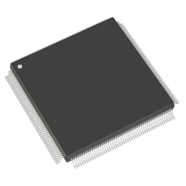
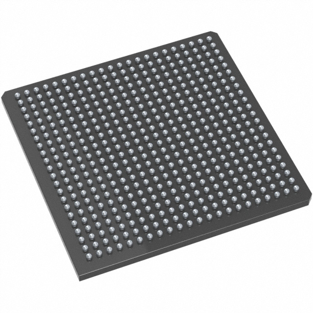
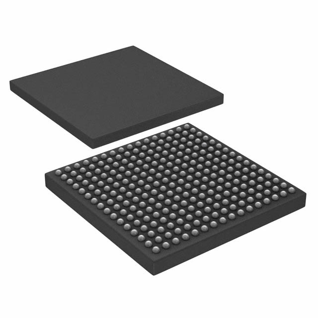
A54SX72A-2FG256
| Part Description |
SX-A Field Programmable Gate Array (FPGA) IC 203 256-BGA |
|---|---|
| Quantity | 315 Available (as of June 15, 2026) |

| Product Category | Field Programmable Gate Array (FPGA) |
|---|---|
| Manufacturer | Microchip Technology |
| Manufacturing Status | Active |
| Manufacturer Standard Lead Time | 12 Weeks |
| Datasheet |
Specifications & Environmental
| Device Package | 256-FPBGA (17x17) | Grade | Commercial | Operating Temperature | 0°C – 70°C | ||
|---|---|---|---|---|---|---|---|
| Package / Case | 256-BGA | Number of I/O | 203 | Voltage | 2.25 V - 5.25 V | ||
| Mounting Method | Surface Mount | RoHS Compliance | RoHS non-compliant | REACH Compliance | REACH Unaffected | ||
| Moisture Sensitivity Level | 3 (168 Hours) | Number of LABs/CLBs | 6036 | Number of Logic Elements/Cells | 6036 | ||
| Number of Gates | 108000 | ECCN | 3A991D | HTS Code | 8542.39.0001 | ||
| Qualification | N/A |
Overview of A54SX72A-2FG256 – SX-A Field Programmable Gate Array (FPGA) IC 203 I/O 256-BGA
The A54SX72A-2FG256 is a member of the SX-A family of nonvolatile, single-chip FPGAs from Microchip Technology. It delivers a programmable logic solution with 108,000 system gates, approximately 6,036 logic elements and up to 2,012 flip-flops in a 256-ball fine-pitch BGA package.
Designed for commercial-grade applications (0 °C to 70 °C), the device supports mixed-voltage operation and configurable I/O, making it suitable for system-level glue logic, interface bridging and PCI-compliant subsystems where deterministic timing, nonvolatile configuration and flexible I/O are required.
Key Features
- Core performance — SX-A family performance figures include up to 250 MHz system performance and 350 MHz internal performance as specified for the family.
- Logic capacity — 108,000 system gates with approximately 6,036 logic elements and support for up to 2,012 dedicated flip-flops for complex custom logic implementations.
- I/O and package — 203 user I/Os in the 256-FPBGA (17×17) fine-pitch BGA package; configurable I/O supports multiple voltage families and mixed-voltage operation.
- Voltage and power — Wide voltage supply range from 2.25 V to 5.25 V enabling 2.5 V, 3.3 V and 5 V mixed-voltage designs with 5 V input tolerance and 5 V drive strength supported by the family.
- Nonvolatile single-chip configuration — Single-chip, nonvolatile architecture removes the need for external configuration memory and supports power-up/power-down friendly operation.
- System interfaces and compliance — Family-level features include 66 MHz PCI compliance and configurable I/O for 3.3 V/5 V PCI, 5 V TTL, 3.3 V LVTTL and 2.5 V LVCMOS2 signaling.
- Reliability and security — Boundary-scan testing compliant with IEEE 1149.1 (JTAG) and Actel Secure Programming Technology with FuseLock™ for protection against reverse engineering.
- Diagnostics and verification — Family supports in-system diagnostic and verification capabilities (Silicon Explorer II) for design validation and troubleshooting.
- Package and mounting — Surface-mount 256-ball fine-pitch BGA (256-FPBGA, 17×17) suitable for compact board designs; RoHS compliant.
- Commercial temperature grade — Rated for operation from 0 °C to 70 °C.
- On-chip memory — Total RAM bits: 0 (no embedded RAM).
Typical Applications
- PCI interface logic — Implements 66 MHz PCI-compliant peripheral or bridge functions using configurable I/O and deterministic timing.
- Mixed-voltage system glue — Bridges between 2.5 V, 3.3 V and 5 V domains with 5 V tolerant inputs and selectable I/O standards.
- Custom protocol and control logic — Deploys complex state machines and timing-critical logic using 108,000 system gates and ~6,036 logic elements.
Unique Advantages
- Nonvolatile, single-chip configuration: Eliminates external configuration storage and simplifies power-up behavior for reliable system bring-up.
- High logic density: 108,000 system gates and ~6,036 logic elements provide the capacity to integrate multiple functions on a single device, reducing BOM count.
- Flexible mixed-voltage I/O: Configurable I/O standards and 5 V tolerance make it straightforward to interface with legacy and modern logic families.
- Security and testability: FuseLock™ secure programming and IEEE 1149.1 boundary-scan support help protect IP and ease manufacturing test.
- Compact, high-pin-count package: 256-FPBGA (17×17) package with 203 I/Os provides density for complex board-level interconnect in a space-efficient footprint.
- Commercial-grade availability: Designed and specified for 0 °C to 70 °C operation with RoHS compliance for standard commercial applications.
Why Choose A54SX72A-2FG256?
The A54SX72A-2FG256 combines a nonvolatile, single-chip FPGA architecture with substantial logic capacity and flexible I/O options to address commercial designs that require deterministic timing, mixed-voltage interfacing and secure, in-system programmability. Its 256-ball fine-pitch BGA package and 203 available I/Os make it a compact yet capable choice for consolidating interface logic and protocol functions onto a single device.
For teams building commercial-grade systems that need a programmable, secure and testable logic element with a wide voltage supply range and family-proven performance features, the A54SX72A-2FG256 provides a clear, verifiable platform to reduce component count and simplify system design.
Request a quote or submit an inquiry to get pricing, availability and technical support information for the A54SX72A-2FG256. Our team can assist with lead times and order placement details.


Date Founded: 1989
Headquarters: Chandler, Arizona, USA
Employees: 22,000+
Revenue: $8.349 Billion
Certifications and Memberships: ISO9001:2015, IATF16949:2016, AS 9100D


