
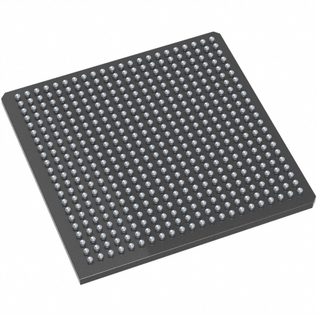
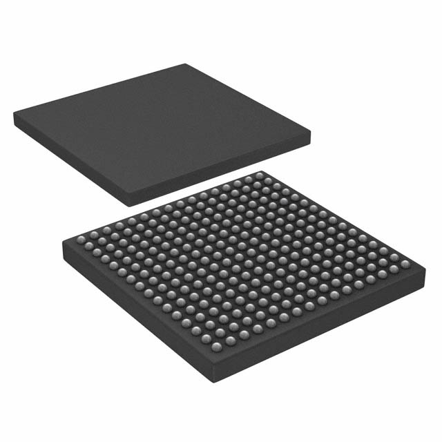
A54SX72A-2FG484
| Part Description |
SX-A Field Programmable Gate Array (FPGA) IC 360 484-BGA |
|---|---|
| Quantity | 1,055 Available (as of June 15, 2026) |

| Product Category | Field Programmable Gate Array (FPGA) |
|---|---|
| Manufacturer | Microchip Technology |
| Manufacturing Status | Active |
| Manufacturer Standard Lead Time | 12 Weeks |
| Datasheet |
Specifications & Environmental
| Device Package | 484-FPBGA (27X27) | Grade | Commercial | Operating Temperature | 0°C – 70°C | ||
|---|---|---|---|---|---|---|---|
| Package / Case | 484-BGA | Number of I/O | 360 | Voltage | 2.25 V - 5.25 V | ||
| Mounting Method | Surface Mount | RoHS Compliance | RoHS non-compliant | REACH Compliance | REACH Unaffected | ||
| Moisture Sensitivity Level | 3 (168 Hours) | Number of LABs/CLBs | 6036 | Number of Logic Elements/Cells | 6036 | ||
| Number of Gates | 108000 | ECCN | 3A991D | HTS Code | 8542.39.0001 | ||
| Qualification | N/A |
Overview of A54SX72A-2FG484 – SX-A Field Programmable Gate Array (FPGA) IC 360 484-BGA
The A54SX72A-2FG484 is an SX-A family FPGA providing a nonvolatile, single-chip programmable solution with up to 108,000 system gates and 6,036 logic elements. It delivers high I/O density—up to 360 user-programmable I/Os—and supports mixed-voltage I/O, making it suitable for designs that require flexible interfacing and high logic capacity.
Designed for commercial-temperature operation (0 °C to 70 °C), the device supports a wide supply range (2.25 V to 5.25 V) and includes features such as hot-swap–compliant I/Os, boundary-scan (JTAG), and Actel Secure Programming Technology (FuseLock™) as documented in the SX-A family datasheet.
Key Features
- Core Performance System and internal performance capability referenced in the SX-A family datasheet (system up to 250 MHz; internal performance up to 350 MHz).
- Logic Capacity 6,036 logic elements and approximately 108,000 system gates to implement medium-to-large FPGA designs, with up to 2,012 dedicated flip-flops available.
- High I/O Count & Clocking Up to 360 user-programmable I/Os, 3 global clocks and 4 quadrant clocks for flexible signal routing and multi-region clocking.
- Configurable I/O Standards Supports configurable I/O for 3.3 V/5 V PCI, 5 V TTL, 3.3 V LVTTL and 2.5 V LVCMOS2, with 5 V input tolerance and 5 V drive strength; enables mixed-voltage operation (2.5 V, 3.3 V, and 5 V).
- Nonvolatile Single-Chip Solution Built-in nonvolatile configuration eliminates the need for external configuration memory and simplifies board-level design.
- Security & Diagnostics Actel Secure Programming Technology with FuseLock™ protects design IP; silicon explorer II in-system diagnostic/verification capability is available per SX-A documentation.
- Power & Hot-Swap Friendly Hot-swap–compliant I/Os and power-up/power-down friendly operation requiring no sequencing of supply voltages.
- Package & Environmental 484-ball fine-pitch BGA (supplier package: 484-FPBGA, 27×27), commercial grade (0 °C to 70 °C), RoHS compliant.
Typical Applications
- PCI and bus-interface systems The device supports 66 MHz PCI compliance and configurable 3.3 V/5 V PCI I/O, enabling use in PCI-based designs and interface bridging.
- Mixed-voltage interface hubs Mixed-voltage I/O support and 5 V input tolerance make the device suitable where multiple logic-voltage domains must be bridged on a single chip.
- Hot-swap and modular systems Hot-swap–compliant I/Os and power-up/power-down friendly behavior suit hot-pluggable modules and backplane-mounted boards.
- Security-sensitive designs FuseLock™ secure programming helps protect intellectual property in applications where design security is important.
Unique Advantages
- High logic density: 6,036 logic elements and 108,000 system gates provide substantial on-chip logic for complex functions without external logic expansion.
- Large, flexible I/O count: Up to 360 user-programmable I/Os accommodate dense peripheral and bus connectivity.
- Nonvolatile, single-chip configuration: Eliminates external configuration flash, simplifying BOMs and board layout.
- Mixed-voltage operation: Support for 2.5 V, 3.3 V and 5 V domains plus 5 V-tolerant inputs enables seamless interfacing across legacy and modern logic levels.
- Design protection and diagnostics: FuseLock™ programming and in-system diagnostic capabilities enhance IP protection and simplify verification.
- Commercial-grade, RoHS compliant: Designed for commercial-temperature applications and compliant with RoHS environmental requirements.
Why Choose A54SX72A-2FG484?
The A54SX72A-2FG484 positions itself as a high-capacity, nonvolatile FPGA for commercial applications that require substantial logic resources and a large number of configurable I/Os. With 6,036 logic elements, up to 360 I/Os, mixed-voltage I/O support, and embedded security features, it offers a compact, single-chip implementation for interface-heavy and IP-sensitive designs.
This device is appropriate for engineering teams seeking a RoHS-compliant, commercial-temperature FPGA with flexible I/O standards, hot-swap capability, and deterministic resources for medium-to-large FPGA designs. The SX-A family documentation and tooling support included in the datasheet help streamline development and verification.
Request a quote or submit an inquiry to our sales team to check availability and pricing for the A54SX72A-2FG484.


Date Founded: 1989
Headquarters: Chandler, Arizona, USA
Employees: 22,000+
Revenue: $8.349 Billion
Certifications and Memberships: ISO9001:2015, IATF16949:2016, AS 9100D


