
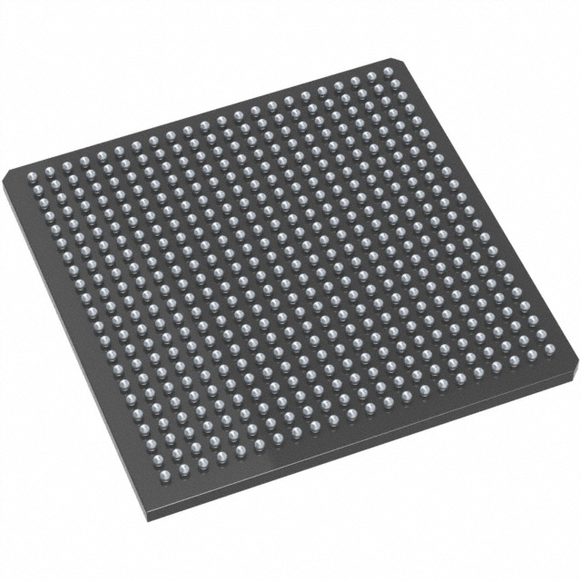
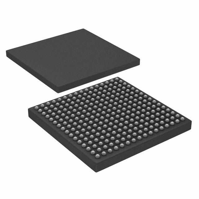
A54SX72A-2FGG484
| Part Description |
SX-A Field Programmable Gate Array (FPGA) IC 360 484-BGA |
|---|---|
| Quantity | 227 Available (as of June 17, 2026) |
| Product Category | Field Programmable Gate Array (FPGA) |
|---|---|
| Manufacturer | Microchip Technology |
| Manufacturing Status | Active |
| Manufacturer Standard Lead Time | 12 Weeks |
| Datasheet |
Specifications & Environmental
| Device Package | 484-FPBGA (27X27) | Grade | Commercial | Operating Temperature | 0°C – 70°C | ||
|---|---|---|---|---|---|---|---|
| Package / Case | 484-BGA | Number of I/O | 360 | Voltage | 2.25 V - 5.25 V | ||
| Mounting Method | Surface Mount | RoHS Compliance | ROHS3 Compliant | REACH Compliance | REACH Unaffected | ||
| Moisture Sensitivity Level | 3 (168 Hours) | Number of LABs/CLBs | 6036 | Number of Logic Elements/Cells | 6036 | ||
| Number of Gates | 108000 | ECCN | 3A991D | HTS Code | 8542.39.0001 | ||
| Qualification | N/A |
Overview of A54SX72A-2FGG484 – SX-A Field Programmable Gate Array (FPGA) IC 360 484-BGA
The A54SX72A-2FGG484 is an SX-A family nonvolatile FPGA offering up to 108,000 system gates and approximately 6,036 logic elements in a 484-ball BGA package. Designed for I/O-dense, mixed-voltage designs, this commercial‑grade device delivers high I/O count and deterministic timing in a single-chip, nonvolatile solution.
With up to 360 user-programmable I/Os, dedicated flip-flops, and hot-swap compliant I/Os, the device addresses designs that require high integration, mixed-voltage interfacing, and in-system diagnostics while operating across a 2.25 V to 5.25 V supply range and a 0 °C to 70 °C commercial temperature window.
Key Features
- Core & Capacity – Up to 108,000 available system gates and approximately 6,036 logic elements, with up to 2,012 dedicated flip-flops for register-intensive designs.
- Performance – Leading-edge performance characteristics documented as up to 250 MHz system performance and up to 350 MHz internal performance for timing-critical logic paths.
- I/O and Mixed-Voltage Support – Up to 360 user-programmable I/O pins; configurable I/O support for 3.3 V / 5 V PCI, 5 V TTL, 3.3 V LVTTL, and 2.5 V LVCMOS2. Supports mixed‑voltage operation with 5 V input tolerance and 5 V drive strength.
- Power and Reliability – Power-up/power-down friendly with no sequencing required for supply voltages; hot-swap compliant I/Os and configurable weak pull-up or pull-down on I/O at power-up.
- Test and Security – Boundary-scan testing compliant with IEEE 1149.1 (JTAG) and Actel Secure Programming Technology with FuseLock™ to protect design IP.
- Package and Mounting – Surface-mount 484-BGA package (supplier device package: 484-FPBGA, 27×27) optimized for compact board integration.
- Commercial Temperature Grade – Rated for 0 °C to 70 °C operation and RoHS compliant.
- System Integration – Deterministic, user-controllable timing, up to 100% resource utilization and pin locking, and in-system diagnostic capability with Silicon Explorer II.
Typical Applications
- PCI Interface and Bridge Logic – 66 MHz PCI compliance and configurable 3.3 V/5 V PCI I/O support make the device suitable for PCI interface and protocol-bridge implementations.
- Mixed‑Voltage I/O Systems – Mixed-voltage operation (2.5 V, 3.3 V, 5 V) and 5 V input tolerance support systems that interconnect logic at differing voltage domains.
- In-System Programmable Logic – Nonvolatile single-chip FPGA architecture with in-system diagnostics is suited to applications that require persistent configuration and board-level verification.
Unique Advantages
- High Logic Density: Up to 108,000 system gates and ~6,036 logic elements provide the capacity to consolidate complex glue logic and mid-size datapaths on a single device, reducing BOM count.
- Extensive I/O: Up to 360 user-programmable I/Os enable direct interfacing to dense peripheral arrays and multiple buses without external I/O expanders.
- Flexible Voltage Handling: Support for mixed 2.5 V, 3.3 V, and 5 V operation with 5 V tolerant inputs permits flexible system-level power architectures.
- Nonvolatile Configuration: Single-chip nonvolatile FPGA removes the need for external configuration memory and simplifies system power sequencing.
- Security and Testability: Built-in FuseLock™ secure programming and IEEE 1149.1 boundary-scan support aid IP protection and board-level test strategies.
- Power-Friendly I/O: Hot-swap compliant I/Os and power-up/power-down friendly operation simplify deployment in systems with complex supply domains.
Why Choose A54SX72A-2FGG484?
The A54SX72A-2FGG484 positions itself as a high-capacity, nonvolatile FPGA for commercial designs that need substantial logic density and a large, flexible I/O complement. Its mixed-voltage support, deterministic timing features, and built-in security and test capabilities make it a practical option for designers consolidating logic, implementing interface bridges, or deploying persistent FPGA configurations without external configuration devices.
With RoHS compliance, a surface-mount 484-BGA footprint, and a commercial operating temperature range, the device provides a balanced combination of integration, performance, and board-level testability for a wide range of commercial embedded applications.
Request a quote or submit an inquiry to get pricing and availability for the A54SX72A-2FGG484 and discuss how this FPGA can fit into your next design.


Date Founded: 1989
Headquarters: Chandler, Arizona, USA
Employees: 22,000+
Revenue: $8.349 Billion
Certifications and Memberships: ISO9001:2015, IATF16949:2016, AS 9100D


