
A54SX72A-2PQG208
| Part Description |
SX-A Field Programmable Gate Array (FPGA) IC 171 208-BFQFP |
|---|---|
| Quantity | 947 Available (as of June 14, 2026) |
| Product Category | Field Programmable Gate Array (FPGA) |
|---|---|
| Manufacturer | Microchip Technology |
| Manufacturing Status | Active |
| Manufacturer Standard Lead Time | 14 Weeks |
| Datasheet |
Specifications & Environmental
| Device Package | 208-PQFP (28x28) | Grade | Commercial | Operating Temperature | 0°C – 70°C | ||
|---|---|---|---|---|---|---|---|
| Package / Case | 208-BFQFP | Number of I/O | 171 | Voltage | 2.25 V - 5.25 V | ||
| Mounting Method | Surface Mount | RoHS Compliance | ROHS3 Compliant | REACH Compliance | REACH Unaffected | ||
| Moisture Sensitivity Level | 3 (168 Hours) | Number of LABs/CLBs | 6036 | Number of Logic Elements/Cells | 6036 | ||
| Number of Gates | 108000 | ECCN | 3A991D | HTS Code | 8542.39.0001 | ||
| Qualification | N/A |
Overview of A54SX72A-2PQG208 – SX-A Field Programmable Gate Array (FPGA) IC, 108k Gates, 171 I/O, 208-BFQFP
The A54SX72A-2PQG208 is a nonvolatile SX-A family FPGA offered in a 208-pin BFQFP surface-mount package. It delivers 108,000 system gates and approximately 6,036 logic elements, making it suitable for commercial embedded applications that require a high-density, nonvolatile programmable logic device.
Built for mixed-voltage systems and in-system configurability, this part targets commercial embedded control, interface bridging and I/O-dense designs where single-chip, nonvolatile FPGA integration, flexible I/O options and secure programming are required.
Key Features
- Core Capacity — 108,000 system gates and 6,036 logic elements with up to 2,012 dedicated flip-flops enable sizable programmable logic and register resources for complex designs.
- Performance — SX-A family performance characteristics include up to 250 MHz system performance and up to 350 MHz internal performance, with this device offered in a –2 speed grade (approximately 25% faster than standard).
- I/O and Mixed‑Voltage Support — 171 user-programmable I/O pins with configurable I/O support for 3.3 V/5 V PCI, 5 V TTL, 3.3 V LVTTL and 2.5 V LVCMOS2; 5 V input tolerance and 5 V drive strength are supported.
- Nonvolatile Single‑Chip Configuration — Single-chip, nonvolatile architecture eliminates the need for external configuration memory.
- Power and Reliability — Power-up/power-down friendly operation with no sequencing required for supply voltages, configurable weak pull-up or pull-down on I/O at power-up, and individual output slew rate control.
- Hot-Swap and Standards — Hot-swap compliant I/Os and 66 MHz PCI compliance for applicable interface implementations.
- Security and Test — Includes Actel Secure Programming Technology with FuseLock™ to protect design IP and supports boundary-scan testing compliant with IEEE 1149.1 (JTAG).
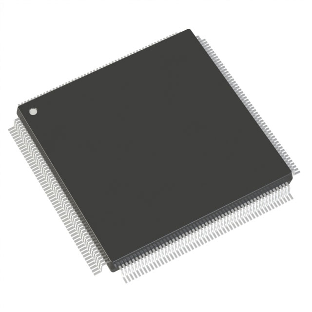
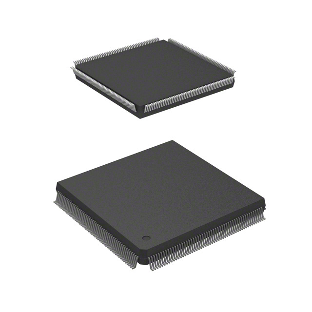
- Package and Mounting — 208‑pin BFQFP (supplier device package listed as 208‑PQFP, 28×28), surface-mount mounting suitable for standard commercial PCB assembly.
- Electrical and Environmental — Voltage supply range 2.25 V to 5.25 V; commercial operating temperature range 0 °C to 70 °C; RoHS compliant.
Typical Applications
- Embedded Control — Implement control logic and state machines where nonvolatile configuration and abundant logic resources are required for commercial devices.
- Interface Bridging — Use mixed-voltage, configurable I/Os and PCI-capable signaling to bridge and adapt between bus standards in I/O-dense systems.
- In-System Diagnostics and Test — Leverage boundary-scan (JTAG) support and in-system diagnostic capabilities for manufacturing test and validation.
- Secure Intellectual Property Protection — Deploy FuseLock™ secure programming to protect proprietary bitstreams in commercial products.
Unique Advantages
- Nonvolatile, single‑chip solution: Eliminates external configuration memory, simplifying board-level BOM and reducing system complexity.
- Flexible mixed‑voltage I/O: Supports multiple I/O standards and 5 V tolerance, enabling direct interfacing with a wide range of legacy and modern peripherals.
- High I/O count in a compact package: 171 user I/Os in a 208-pin BFQFP provide dense connectivity without requiring larger packages.
- Secure programming: FuseLock™ technology helps protect design IP and mitigate reverse engineering risks.
- Power sequencing robustness: Power-up/power-down friendly operation avoids complex supply sequencing requirements during system design and deployment.
- Deterministic timing and control: Individual output slew control and configurable pull resistors provide predictable signal integrity and startup behavior.
Why Choose A54SX72A-2PQG208?
The A54SX72A-2PQG208 offers a high-capacity, nonvolatile FPGA solution tailored for commercial embedded applications that need substantial logic resources, flexible mixed-voltage I/O and on-chip security. Its 108k system gates, roughly 6,036 logic elements and 171 I/Os in a 208‑pin BFQFP package deliver a balance of integration density and connectivity for complex, I/O-heavy designs.
With hot-swap capable I/Os, power-up friendly operation, boundary-scan support and FuseLock™ secure programming, this device provides a stable platform for designs prioritizing in-field configurability, testability and IP protection, while operating across a broad 2.25 V to 5.25 V supply range in commercial temperature environments.
Request a quote or submit an inquiry to receive pricing and availability information for the A54SX72A-2PQG208.


Date Founded: 1989
Headquarters: Chandler, Arizona, USA
Employees: 22,000+
Revenue: $8.349 Billion
Certifications and Memberships: ISO9001:2015, IATF16949:2016, AS 9100D


