
A54SX72A-CQ208
| Part Description |
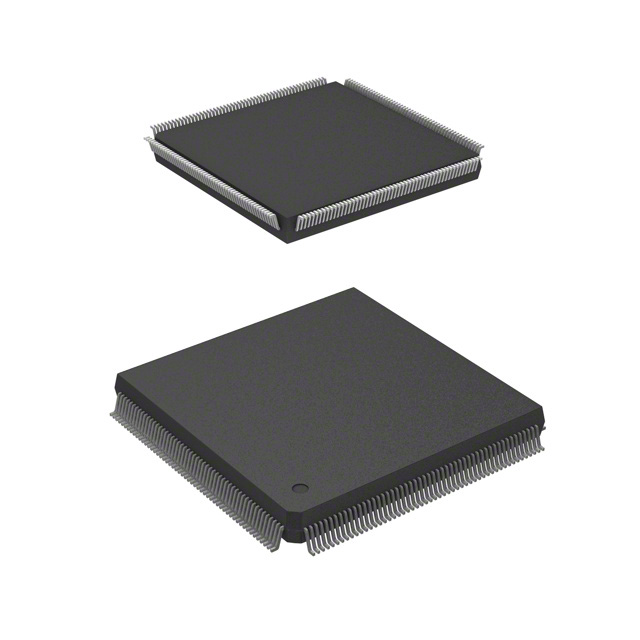
SX-A Field Programmable Gate Array (FPGA) IC 171 208-BFCQFP with Tie Bar |
|---|---|
| Quantity | 943 Available (as of June 18, 2026) |

| Product Category | Field Programmable Gate Array (FPGA) |
|---|---|
| Manufacturer | Microchip Technology |
| Manufacturing Status | Active |
| Manufacturer Standard Lead Time | 36 Weeks |
| Datasheet |
Specifications & Environmental
| Device Package | 208-CQFP (75x75) | Grade | Commercial | Operating Temperature | 0°C – 70°C | ||
|---|---|---|---|---|---|---|---|
| Package / Case | 208-BFCQFP with Tie Bar | Number of I/O | 171 | Voltage | 2.25 V - 5.25 V | ||
| Mounting Method | Surface Mount | RoHS Compliance | RoHS non-compliant | REACH Compliance | REACH Unaffected | ||
| Moisture Sensitivity Level | 3 (168 Hours) | Number of LABs/CLBs | 6036 | Number of Logic Elements/Cells | 6036 | ||
| Number of Gates | 108000 | ECCN | 3A991D | HTS Code | 8542.39.0001 | ||
| Qualification | N/A |
Overview of A54SX72A-CQ208 – SX-A Field Programmable Gate Array (FPGA) IC 171 208-BFCQFP with Tie Bar
The A54SX72A-CQ208 is a commercial-grade SX-A family FPGA from Microchip Technology supplied in a 208‑pin BFCQFP package with tie bar. It delivers a high-capacity, fixed-architecture FPGA option with 108,000 system gates and 6,036 logic elements for custom logic integration and board-level programmable functions.
Designed for applications requiring flexible I/O and mixed-voltage support, the device provides up to 171 user-programmable I/Os, a wide supply range (2.25 V to 5.25 V), and standard commercial operating temperature support (0 °C to 70 °C).
Key Features
- Capacity and Logic — 108,000 system gates and 6,036 logic elements (combinatorial cells and logic modules) for complex glue logic, protocol handling, and custom datapaths.
- I/O and Voltage Flexibility — Up to 171 user-programmable I/Os in the 208‑pin package; device-level voltage supply range of 2.25 V to 5.25 V and family-level mixed-voltage I/O support.
- Performance — Documented device timing includes a 6.7 ns clock‑to‑out (pin‑to‑pin) figure for the A54SX72A device and multiple on-chip clock resources (3 global clocks, 4 quadrant clocks) to support synchronous designs.
- Memory — No dedicated on‑chip RAM bits (Total Ram Bits: 0), making the device suited to designs emphasizing combinatorial and registered logic elements rather than embedded RAM.
- Package and Mounting — 208‑BFCQFP with tie bar, surface‑mount; supplier package listed as 208‑CQFP (75×75).
- Standards and Test Support — Family-level features include boundary-scan testing (IEEE 1149.1 JTAG) and power-up/power-down friendly operation (no supply sequencing required), as documented in the product family datasheet.
- Compliance — RoHS compliant.
Typical Applications
- Embedded systems and control logic — Implement custom control, state machines, and protocol logic using 6,036 logic elements and up to 171 I/Os for board-level integration.
- Mixed‑voltage interface bridging — Use the device’s wide supply range and family-level mixed-voltage I/O support to interface between 2.5 V, 3.3 V and 5 V domains on a single chip.
- PCI and legacy bus interfacing — Family documentation indicates support for 3.3 V / 5 V PCI signaling, enabling use in systems that require legacy bus compatibility.
- Prototyping and system integration — High gate count and plentiful I/O make the device suitable for system prototypes and consolidating multiple discrete logic functions into a single FPGA.
Unique Advantages
- High logic capacity: 108,000 system gates and 6,036 logic elements provide headroom for complex state machines, glue logic, and protocol accelerators.
- Flexible I/O and voltage range: Up to 171 user I/Os and a 2.25 V to 5.25 V supply range simplify integration with mixed-voltage system components.
- Deterministic timing resources: Multiple global and quadrant clocks and documented clock‑to‑out timing (6.7 ns) support predictable synchronous design.
- Board-level packaging: 208‑pin BFCQFP surface-mount package with tie bar offers a standardized footprint for high-density board designs.
- Testability and integration: Boundary-scan support and power-up/power-down friendly behavior (family-level) help streamline manufacturing test and system bring-up.
- Regulatory compliance: RoHS compliant for designs requiring restricted‑substance conformance.
Why Choose A54SX72A-CQ208?
The A54SX72A-CQ208 is positioned for designers who need a commercially graded, high‑capacity FPGA with extensive I/O and flexible voltage operation. With 108,000 system gates and 6,036 logic elements in a 208‑pin BFCQFP package, the device lets you consolidate discrete logic, implement protocol interfaces, and bridge multiple voltage domains on a single component.
Its combination of capacity, documented timing primitives, and board-ready package make it a practical choice for embedded system integrators, prototype development, and applications where predictable timing and flexible I/O are priorities. RoHS compliance and surface-mount packaging support modern assembly and regulatory requirements.
Request a quote or submit a product inquiry for pricing and availability of the A54SX72A-CQ208.


Date Founded: 1989
Headquarters: Chandler, Arizona, USA
Employees: 22,000+
Revenue: $8.349 Billion
Certifications and Memberships: ISO9001:2015, IATF16949:2016, AS 9100D


