
A54SX72A-2FG256I
| Part Description |
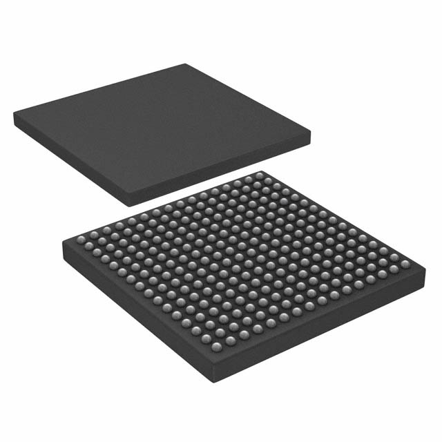
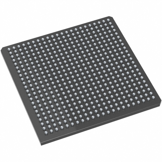
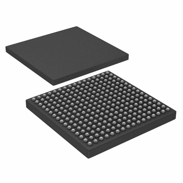
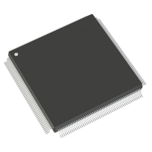
SX-A Field Programmable Gate Array (FPGA) IC 203 256-BGA |
|---|---|
| Quantity | 301 Available (as of October 8, 2026) |
| Product Category | Field Programmable Gate Array (FPGA) |
|---|---|
| Manufacturer | Microchip Technology |
| Manufacturing Status | Active |
| Manufacturer Standard Lead Time | 12 Weeks |
| Datasheet |
Specifications & Environmental
| Device Package | 256-FPBGA (17x17) | Grade | Industrial | Operating Temperature | -40°C – 85°C | ||
|---|---|---|---|---|---|---|---|
| Package / Case | 256-BGA | Number of I/O | 203 | Voltage | 2.25 V - 5.25 V | ||
| Mounting Method | Surface Mount | RoHS Compliance | RoHS non-compliant | REACH Compliance | REACH Unaffected | ||
| Moisture Sensitivity Level | 3 (168 Hours) | Number of LABs/CLBs | 6036 | Number of Logic Elements/Cells | 6036 | ||
| Number of Gates | 108000 | ECCN | 3A991D | HTS Code | 8542.39.0001 | ||
| Qualification | N/A |
Overview of A54SX72A-2FG256I – SX-A Field Programmable Gate Array (FPGA) IC 203 I/O, 256-BGA
The A54SX72A-2FG256I is an SX-A family FPGA from Microchip Technology offering a nonvolatile, single-chip programmable solution for industrial designs. It combines a high-capacity logic fabric with a large I/O count and mixed-voltage I/O support to address glue-logic, protocol bridging and control applications that require deterministic timing and in-system diagnostics.
Key value propositions include 108,000 system gates of capacity implemented as 6,036 logic elements, up to 203 user I/Os in a 256-pin FBGA package, and industrial temperature operation for robust deployed systems.
Key Features
- Core capacity and performance — 108,000 system gates implemented as 6,036 logic elements; family-level performance figures include up to 250 MHz system performance and up to 350 MHz internal performance as documented for the SX-A family.
- Logic and flip-flops — Supports up to 2,012 dedicated flip-flops (family specification) enabling register-rich designs and synchronous implementations.
- I/O flexibility — 203 user-programmable I/Os with configurable I/O support for 3.3 V / 5 V PCI, 5 V TTL, 3.3 V LVTTL and 2.5 V LVCMOS2 levels, hot-swap compliant I/Os, and 5 V input tolerance and 5 V drive strength (family features).
- Memory — No on-chip RAM (Total RAM bits: 0) as provided in the product data.
- Power and sequencing — Operates from a 2.25 V to 5.25 V supply range and is power-up/power-down friendly with no sequencing required for supply voltages (family feature).
- Package and mounting — 256-BGA package (supplier package: 256-FPBGA, 17×17 mm), surface-mount mounting suitable for compact, board-level integration.
- Industrial temperature grade — Rated for operation from −40 °C to +85 °C.
- Security and test — Supports boundary-scan testing in compliance with IEEE 1149.1 (JTAG) and includes Actel Secure Programming Technology with FuseLock for design protection; also offers in-system diagnostics and verification capability with Silicon Explorer II (family features).
- Deterministic timing — Deterministic, user-controllable timing for predictable system behavior (family feature).
- Standards and compatibility — 66 MHz PCI compliant (family feature), enabling use in PCI-based subsystems where applicable.
- RoHS status — RoHS compliant.
Typical Applications
- Industrial control and automation — Industrial temperature rating (−40 °C to +85 °C) and a broad supply range (2.25 V–5.25 V) make this FPGA suitable for control logic, motor drives and factory automation interfaces.
- Protocol bridging and interface logic — High I/O count (203 I/Os) and configurable multi-voltage I/O support enable protocol translation, bus bridging and custom peripheral interfacing.
- PCI-based subsystems — 66 MHz PCI compliance and deterministic timing support implementation of PCI glue logic and interface controllers within larger systems.
- Secure and verifiable systems — Built-in secure programming (FuseLock) and JTAG boundary-scan support are suited to applications that require IP protection and in-system testability.
Unique Advantages
- High-capacity programmable fabric: 108,000 system gates and 6,036 logic elements deliver substantial logic resources for complex glue logic and custom functions without adding discrete ASICs.
- Large, flexible I/O: 203 user I/Os with mixed-voltage support reduce the need for level shifters and simplify board-level interfacing to diverse peripherals and buses.
- Nonvolatile single-chip solution: On-chip nonvolatile configuration removes the requirement for external configuration memory and simplifies system design.
- Industrial robustness: Surface-mount 256-FPBGA package plus industrial temperature rating supports deployment in harsh environments.
- Security and testability: FuseLock secure programming and IEEE 1149.1 boundary-scan deliver IP protection and standardized manufacturing/test support.
- Predictable timing behavior: Deterministic, user-controllable timing helps achieve consistent system-level performance and simplifies timing closure.
Why Choose A54SX72A-2FG256I?
The A54SX72A-2FG256I positions itself as a high-capacity, secure SX-A family FPGA for industrial designs that require a combination of large logic resources, extensive I/O and predictable timing. Its nonvolatile single-chip architecture and mixed-voltage I/O support simplify BOM and board design while the industrial temperature rating broadens deployment options.
This device is well suited to engineers building protocol bridges, PCI subsystem logic, secure embedded controllers and other applications where robust I/O, in-system testability and design protection are priorities. Choosing this part supports scalability within the SX-A family and leverages family-level features such as in-system diagnostics and secure programming.
Request a quote or contact sales to discuss your design requirements and obtain pricing and availability information for the A54SX72A-2FG256I.





















Date Founded: 1989
Headquarters: Chandler, Arizona, USA
Employees: 22,000+
Revenue: $8.349 Billion
Certifications and Memberships: ISO9001:2015, IATF16949:2016, AS 9100D




