
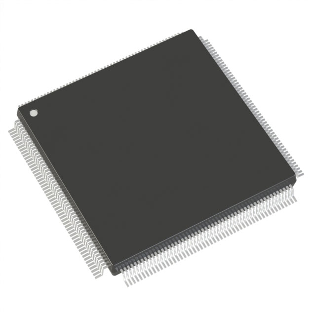
A54SX72A-FPQ208
| Part Description |
SX-A Field Programmable Gate Array (FPGA) IC 171 208-BFQFP |
|---|---|
| Quantity | 565 Available (as of June 15, 2026) |

| Product Category | Field Programmable Gate Array (FPGA) |
|---|---|
| Manufacturer | Microchip Technology |
| Manufacturing Status | Obsolete |
| Manufacturer Standard Lead Time | Contact Us |
| Datasheet |
Specifications & Environmental
| Device Package | 208-PQFP (28x28) | Grade | Commercial | Operating Temperature | 0°C – 70°C | ||
|---|---|---|---|---|---|---|---|
| Package / Case | 208-BFQFP | Number of I/O | 171 | Voltage | 2.25 V - 5.25 V | ||
| Mounting Method | Surface Mount | RoHS Compliance | RoHS non-compliant | REACH Compliance | REACH Unaffected | ||
| Moisture Sensitivity Level | 3 (168 Hours) | Number of LABs/CLBs | 6036 | Number of Logic Elements/Cells | 6036 | ||
| Number of Gates | 108000 | ECCN | 3A991D | HTS Code | 8542.39.0001 | ||
| Qualification | N/A |
Overview of A54SX72A-FPQ208 – SX-A FPGA, 108,000 System Gates, 171 I/O, 208‑pin BFQFP
The A54SX72A-FPQ208 is a member of the SX‑A family Field Programmable Gate Array (FPGA) from Microchip Technology. It is a nonvolatile, single‑chip FPGA delivering 108,000 system gates and approximately 6,036 logic elements for mid‑to‑high complexity logic integration.
Designed for applications that require mixed‑voltage I/O and robust system performance, the device combines high logic capacity with configurable I/O, deterministic timing features and built‑in security mechanisms to support embedded and PCI‑compatible designs within a commercial 0 °C to 70 °C temperature range.
Key Features
- Core Performance System performance up to 250 MHz and internal performance up to 350 MHz as specified for the SX‑A family.
- Logic Capacity 108,000 system gates with approximately 6,036 logic elements and up to 4,024 flip‑flops for complex combinatorial and sequential logic.
- I/O and Interface Support 171 user‑programmable I/Os with configurable support for 3.3 V/5 V PCI, 5 V TTL, 3.3 V LVTTL and 2.5 V LVCMOS2. I/Os include 5 V input tolerance and 5 V drive capability where supported.
- Nonvolatile Architecture & Security Single‑chip nonvolatile configuration with Actel Secure Programming Technology (FuseLock™) to prevent reverse engineering and protect IP.
- Power and Reliability Wide supply voltage range from 2.25 V to 5.25 V, hot‑swap compliant I/Os and power‑up/power‑down friendly operation (no supply sequencing required).
- System Test and Diagnostics Boundary‑scan testing (IEEE 1149.1 JTAG) and deterministic, user‑controllable timing enable in‑system test and verification.
- Packaging and Temperature Surface‑mount 208‑pin package (listed as 208‑BFQFP; supplier device package: 208‑PQFP 28×28) and commercial operating range 0 °C to 70 °C. RoHS compliant.
- Family Capabilities Supports up to 100% resource utilization and 100% pin locking as described for the SX‑A family devices.
Typical Applications
- PCI‑Compatible Systems Use the device’s 66 MHz PCI compliance and configurable 5 V/3.3 V I/O options to implement PCI interfaces and bridging logic.
- Mixed‑Voltage Embedded Designs Ideal where multiple I/O standards and 5 V tolerance are required for interfacing legacy and modern peripherals.
- In‑System Programmable Logic Nonvolatile single‑chip configuration and built‑in security make it suitable for embedded control and protected IP implementations.
Unique Advantages
- Highly integrated logic capacity: 108,000 system gates and ~6,036 logic elements reduce the need for external glue logic and simplify board design.
- Flexible mixed‑voltage I/O: Configurable I/O standards and 5 V tolerance support a wide range of peripheral interfaces without additional level shifters.
- Nonvolatile, secure configuration: Single‑chip nonvolatile architecture with FuseLock™ technology protects designs and removes external configuration components.
- Robust system performance: 250 MHz system and 350 MHz internal performance characteristics support demanding timing requirements.
- Design for testability: Boundary‑scan (IEEE 1149.1) and deterministic timing facilitate in‑system test, verification and debugging.
- Wide supply range and power friendliness: 2.25 V to 5.25 V operation with no required sequencing simplifies power rail design and hot‑swap scenarios.
Why Choose A54SX72A-FPQ208?
The A54SX72A-FPQ208 is positioned for designs that need substantial programmable logic, flexible mixed‑voltage I/O and nonvolatile, secure configuration in a commercial‑grade FPGA. With 108,000 system gates, approximately 6,036 logic elements and 171 user I/Os, it addresses mid‑ to high‑complexity integration tasks while supporting PCI‑compatible interfaces and deterministic timing control.
Its combination of performance, configurable I/O and security features delivers long‑term value for embedded system designers seeking a compact, single‑chip FPGA solution that minimizes external components and supports in‑system testing and verification.
Request a quote or submit a procurement inquiry to get pricing, availability and lead‑time information for the A54SX72A-FPQ208.


Date Founded: 1989
Headquarters: Chandler, Arizona, USA
Employees: 22,000+
Revenue: $8.349 Billion
Certifications and Memberships: ISO9001:2015, IATF16949:2016, AS 9100D


