
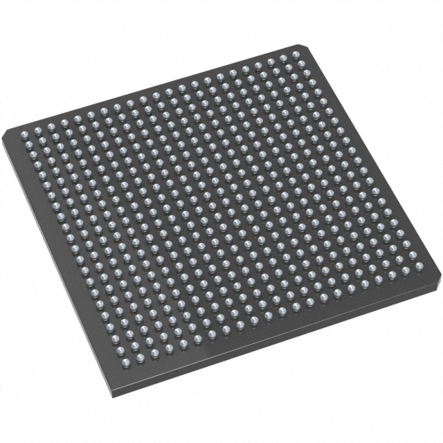
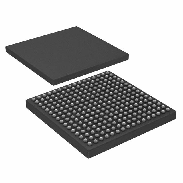
A54SX72A-FGG484I
| Part Description |
SX-A Field Programmable Gate Array (FPGA) IC 360 484-BGA |
|---|---|
| Quantity | 385 Available (as of June 18, 2026) |

| Product Category | Field Programmable Gate Array (FPGA) |
|---|---|
| Manufacturer | Microchip Technology |
| Manufacturing Status | Active |
| Manufacturer Standard Lead Time | 12 Weeks |
| Datasheet |
Specifications & Environmental
| Device Package | 484-FPBGA (27X27) | Grade | Industrial | Operating Temperature | -40°C – 85°C | ||
|---|---|---|---|---|---|---|---|
| Package / Case | 484-BGA | Number of I/O | 360 | Voltage | 2.25 V - 5.25 V | ||
| Mounting Method | Surface Mount | RoHS Compliance | ROHS3 Compliant | REACH Compliance | REACH Unaffected | ||
| Moisture Sensitivity Level | 3 (168 Hours) | Number of LABs/CLBs | 6036 | Number of Logic Elements/Cells | 6036 | ||
| Number of Gates | 108000 | ECCN | 3A991D | HTS Code | 8542.39.0001 | ||
| Qualification | N/A |
Overview of A54SX72A-FGG484I – SX-A Field Programmable Gate Array (FPGA) IC, 360 I/O, 484-BGA
The A54SX72A-FGG484I is an SX-A family FPGA device offered in a 484-pin fine-pitch BGA package. It provides a nonvolatile, single-chip FPGA architecture with up to 108,000 system gates and support for up to 360 user-programmable I/Os.
Designed for industrial-temperature operation, this device combines deterministic timing, hot-swap–compliant I/Os, and mixed-voltage I/O support to address board-level designs that require flexible I/O, secure configuration, and in-system diagnostics.
Key Features
- Core Performance — SX-A family performance characteristics cited in the datasheet include system performance up to 250 MHz and internal performance up to 350 MHz.
- Logic Capacity — Approximately 108,000 system gates and 6,036 logic elements provide substantial combinatorial and sequential resources for complex logic implementations.
- Flip-Flop Resources — Device supports up to 2,012 dedicated flip-flops for register-rich designs.
- I/O and Mixed-Voltage Support — Up to 360 user-programmable I/Os with configurable support for 3.3 V / 5 V PCI, 5 V TTL, 3.3 V LVTTL, and 2.5 V LVCMOS2; supports mixed-voltage operation with 5 V input tolerance and 5 V drive strength.
- Power and Configuration — Nonvolatile, single-chip configuration (no external configuration memory required) and power-up/power-down friendly operation without supply sequencing.
- Reliability & Testing — Boundary-scan testing compliant with IEEE 1149.1 (JTAG) and hot-swap–compliant I/Os for modular systems.
- Security — Includes Actel Secure Programming Technology with FuseLock™ to prevent reverse engineering and protect design IP (as documented for the SX-A family).
- Package & Mounting — Surface-mount 484-FPBGA package (27×27) suitable for compact board layouts; supplier device package listed as 484-FPBGA (27X27).
- Voltage and Temperature — Operates from 2.25 V to 5.25 V and rated for industrial temperature operation from −40 °C to +85 °C.
- Environmental — RoHS compliant packaging.
Typical Applications
- PCI and Bus-Based Expansion Cards — Configurable I/O support for 3.3 V / 5 V PCI and 66 MHz PCI compliance enable use on PCI-based add-in cards and bus interface logic.
- Modular, Hot-Swap Systems — Hot-swap–compliant I/Os and power-up/power-down–friendly behavior suit modular boards and hot-pluggable subsystems.
- Secure Embedded Systems — Nonvolatile single-chip configuration combined with FuseLock™ secure programming supports applications requiring design protection.
- In-System Test and Verification — Boundary-scan (IEEE 1149.1) and in-system diagnostic capabilities enable board-level test and verification workflows.
Unique Advantages
- High Logic Density: With approximately 6,036 logic elements and 108,000 system gates, the device supports complex logic integration on a single chip, reducing external glue logic.
- Extensive I/O Flexibility: Up to 360 user I/Os with mixed-voltage support and 5 V tolerance allow direct interfacing to a wide range of legacy and modern I/O standards.
- Nonvolatile Single-Chip Configuration: Eliminates the need for external configuration memory, simplifying BOM and system startup behavior.
- Industrial Temperature Rating: Rated for −40 °C to +85 °C operation for deployment in industrial environments where extended temperature range is required.
- Built-In Security and Testability: FuseLock™ secure programming and IEEE 1149.1 boundary-scan support protect IP and simplify manufacturing test and field diagnostics.
- RoHS Compliant Packaging: Meets RoHS requirements for environmentally conscious designs.
Why Choose A54SX72A-FGG484I?
The A54SX72A-FGG484I positions itself as a high-capacity, industrial-temperature SX-A family FPGA with robust I/O flexibility, on-chip nonvolatile configuration, and integrated security and test features. Its combination of approximately 6,036 logic elements, up to 360 user I/Os, and dedicated flip-flop resources makes it suitable for board-level designs that require substantial programmable logic, mixed-voltage interfacing, and deterministic timing.
For engineering teams targeting industrial applications that benefit from single-chip nonvolatile configuration, hot-swap I/O capability, and built-in design protection, this device delivers a clear, verifiable specification set and packaging suitable for compact, surface-mount designs.
Request a quote or submit an inquiry to receive pricing and availability for the A54SX72A-FGG484I. Provide your quantity and lead-time requirements to get a tailored response.


Date Founded: 1989
Headquarters: Chandler, Arizona, USA
Employees: 22,000+
Revenue: $8.349 Billion
Certifications and Memberships: ISO9001:2015, IATF16949:2016, AS 9100D


