
A54SX72A-FGG256M
| Part Description |
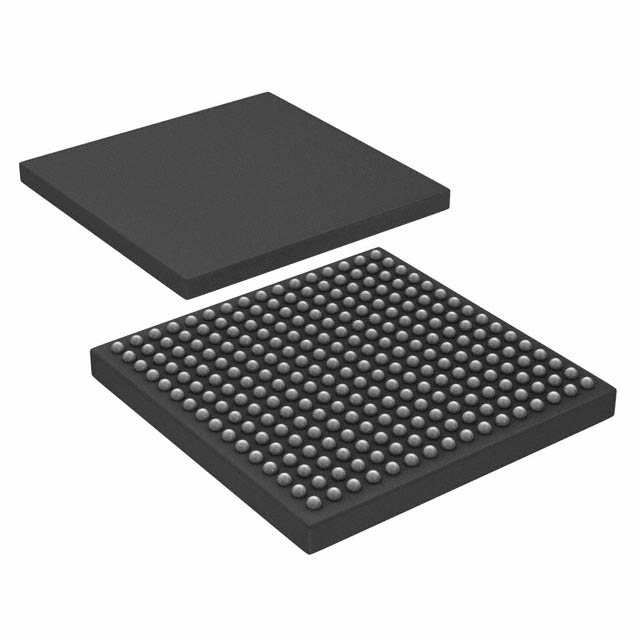
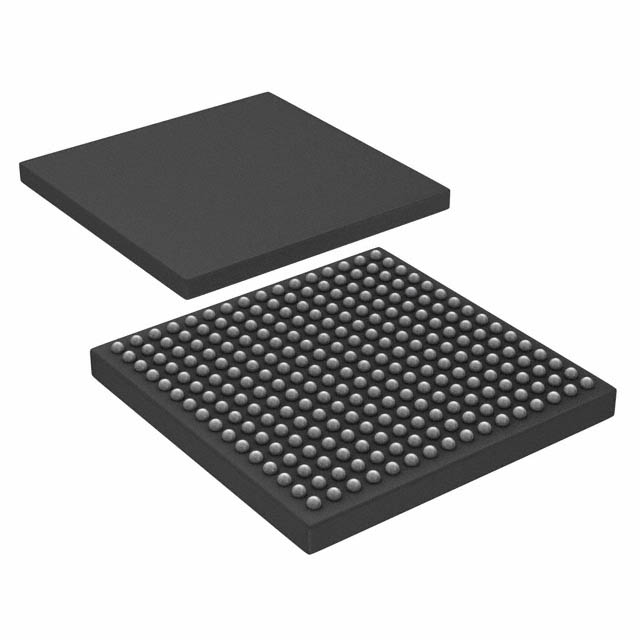
SX-A Field Programmable Gate Array (FPGA) IC 203 256-BGA |
|---|---|
| Quantity | 315 Available (as of October 7, 2026) |
| Product Category | Field Programmable Gate Array (FPGA) |
|---|---|
| Manufacturer | Microchip Technology |
| Manufacturing Status | Active |
| Manufacturer Standard Lead Time | 20 Weeks |
| Datasheet |
Specifications & Environmental
| Device Package | 256-FPBGA (17x17) | Grade | Military | Operating Temperature | -55°C – 125°C | ||
|---|---|---|---|---|---|---|---|
| Package / Case | 256-BGA | Number of I/O | 203 | Voltage | 2.25 V - 5.25 V | ||
| Mounting Method | Surface Mount | RoHS Compliance | ROHS3 Compliant | REACH Compliance | REACH Unaffected | ||
| Moisture Sensitivity Level | 3 (168 Hours) | Number of LABs/CLBs | 6036 | Number of Logic Elements/Cells | 6036 | ||
| Number of Gates | 108000 | ECCN | 3A001A2C | HTS Code | 8542.39.0001 | ||
| Qualification | N/A |
Overview of A54SX72A-FGG256M – SX-A Field Programmable Gate Array, 203 I/O, 256‑BGA
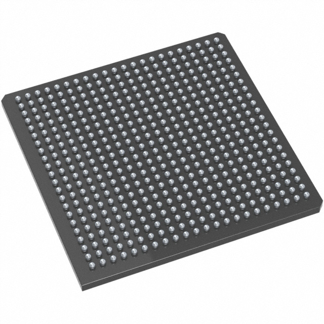
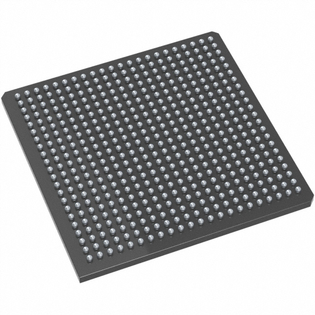
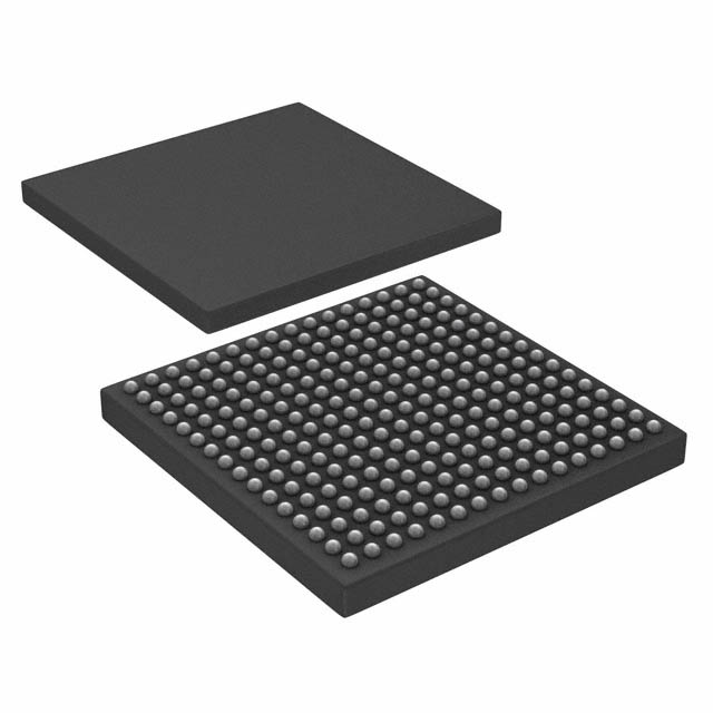
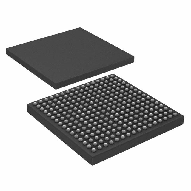
The A54SX72A-FGG256M is a military‑grade SX-A family FPGA in a 256‑ball fine‑pitch BGA (17×17) package, offering high logic capacity and a large I/O count for rugged, temperature‑extreme applications. It provides a nonvolatile, single‑chip FPGA architecture targeted at systems requiring deterministic timing, secure configuration, and extensive programmable I/O.
With 108,000 system gates, 6,036 logic elements, and 203 user I/Os, this device addresses applications that demand high gate density, flexible mixed‑voltage I/O support, and operation across a wide supply and temperature range.
Key Features
- Logic Capacity 108,000 system gates and 6,036 logic elements provide substantial on‑chip logic resources for complex designs.
- User I/O 203 programmable I/Os support configurable drive and input standards to interface with a variety of external devices.
- Performance Documented family performance includes up to 250 MHz system performance and up to 350 MHz internal performance for timing‑sensitive designs.
- Nonvolatile, Single‑Chip Design On‑chip nonvolatile configuration removes the need for external configuration memory and simplifies board-level design.
- I/O Flexibility & PCI Support Configurable I/O supports 3.3 V / 5 V PCI, 5 V TTL, 3.3 V LVTTL and 2.5 V LVCMOS2; 66 MHz PCI compliance is supported.
- Mixed‑Voltage Operation Supports 2.5 V, 3.3 V and 5 V mixed‑voltage operation with 5 V input tolerance and 5 V drive strength.
- Security & Testability Includes Actel Secure Programming Technology with FuseLock™ to protect designs and IEEE 1149.1 JTAG boundary‑scan compliance for board‑level test.
- System Reliability Hot‑swap compliant I/Os and power‑up/power‑down friendly operation (no supply sequencing required) aid robust system integration.
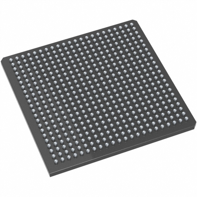
- Package & Mounting 256‑ball fine‑pitch BGA (256‑FPBGA, 17×17) in a surface‑mount form factor suitable for compact, high‑density PCBs.
- Rugged Temperature Range Military temperature grade operation from −55°C to 125°C for deployments in extreme environments.
- Supply Voltage Range Wide supply tolerance from 2.25 V to 5.25 V to accommodate mixed power architectures.
- Diagnostic & Development Support In‑system diagnostic and verification capability is available via Silicon Explorer II (as documented for the SX‑A family).
Typical Applications
- Military and Aerospace Systems Military temperature grade and robust I/O/power characteristics make this FPGA suitable for defense electronics and avionics subsystems.
- Secure Embedded Controllers Nonvolatile configuration and FuseLock™ programming help protect IP and support secure embedded control applications.
- PCI‑Based Systems and Peripherals 66 MHz PCI compliance and multi‑voltage I/O support allow integration into PCI host or peripheral designs.
- High‑Density Logic Integration High gate count and 6,036 logic elements enable consolidation of multiple functions into a single device to reduce BOM and board complexity.
Unique Advantages
- High Integration Density: 108,000 system gates and 6,036 logic elements reduce the need for multiple devices, saving board space and BOM costs.
- Wide Voltage Flexibility: 2.25 V to 5.25 V supply range and mixed‑voltage I/O support simplify interfacing with legacy and modern logic families.
- Military Temperature Rating: Rated for −55°C to 125°C, enabling reliable operation in harsh and mission‑critical environments.
- Nonvolatile Single‑Chip Configuration: Eliminates external configuration memory, improving system reliability and startup behavior.
- Built‑In Security & Test Features: FuseLock™ programming and IEEE 1149.1 JTAG boundary‑scan support add design protection and streamlined board testing.
- Hot‑Swap and Power‑Friendly I/Os: Power‑up/power‑down friendliness and hot‑swap compliance help integrate the FPGA into systems with complex power sequencing or hot‑replace requirements.
Why Choose A54SX72A-FGG256M?
The A54SX72A-FGG256M combines high logic capacity, broad I/O flexibility and military‑grade environmental performance in a compact 256‑ball FG BGA package. Its nonvolatile, single‑chip architecture and security features make it suitable for designs that require robust configuration handling and protection against reverse engineering.
This device is well suited for engineers building compact, high‑functionality systems where long‑term reliability, deterministic timing and wide operating ranges are essential. Its combination of gate density, I/O count and stringent temperature rating provides a scalable platform for defense, secure embedded and PCI‑oriented applications.
Request a quote or submit a purchase inquiry for the A54SX72A-FGG256M to discuss availability and pricing for your project.





















Date Founded: 1989
Headquarters: Chandler, Arizona, USA
Employees: 22,000+
Revenue: $8.349 Billion
Certifications and Memberships: ISO9001:2015, IATF16949:2016, AS 9100D




