
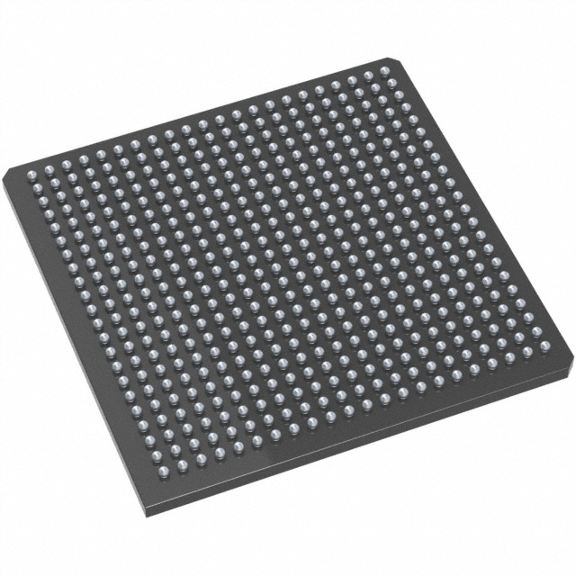
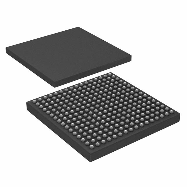
A54SX72A-FG484M
| Part Description |
SX-A Field Programmable Gate Array (FPGA) IC 360 484-BGA |
|---|---|
| Quantity | 1,760 Available (as of June 15, 2026) |
| Product Category | Field Programmable Gate Array (FPGA) |
|---|---|
| Manufacturer | Microchip Technology |
| Manufacturing Status | Active |
| Manufacturer Standard Lead Time | 20 Weeks |
| Datasheet |
Specifications & Environmental
| Device Package | 484-FPBGA (27X27) | Grade | Military | Operating Temperature | -55°C – 125°C | ||
|---|---|---|---|---|---|---|---|
| Package / Case | 484-BGA | Number of I/O | 360 | Voltage | 2.25 V - 5.25 V | ||
| Mounting Method | Surface Mount | RoHS Compliance | RoHS non-compliant | REACH Compliance | REACH Unaffected | ||
| Moisture Sensitivity Level | 3 (168 Hours) | Number of LABs/CLBs | 6036 | Number of Logic Elements/Cells | 6036 | ||
| Number of Gates | 108000 | ECCN | 3A001A2C | HTS Code | 8542.39.0001 | ||
| Qualification | N/A |
Overview of A54SX72A-FG484M – SX-A Field Programmable Gate Array (FPGA) IC 360 484-BGA
The A54SX72A-FG484M is a military-grade SX-A family Field Programmable Gate Array (FPGA) offered by Microchip Technology. This nonvolatile, single-chip FPGA delivers high logic capacity and dense I/O for applications that require secure, in-system programmability and robust operation across a wide temperature range.
Designed for systems needing high I/O count, deterministic timing and secure programming, the device targets mission-critical and rugged electronic designs where long-term reliability and configurability are essential.
Key Features
- Logic Capacity — 108,000 system gates and approximately 6,036 logic elements (combinatorial cells) provide substantial on-chip programmable logic resources.
- I/O and Interfaces — Up to 360 user-programmable I/O pins with configurable support for 3.3 V/5 V PCI, 5 V TTL, 3.3 V LVTTL and 2.5 V LVCMOS2 signaling. I/Os are hot-swap compliant and offer configurable weak pull-up or pull-down at power-up.
- Performance — Datasheet-specified system performance up to 250 MHz and internal performance up to 350 MHz, with deterministic, user-controllable timing for predictable system behaviour.
- Power and Voltage Flexibility — Operates from 2.25 V to 5.25 V and provides 5 V input tolerance with 5 V drive strength where supported, enabling mixed-voltage designs.
- Package and Mechanical — 484-FPBGA package (27×27 mm) providing a fine-pitch BGA footprint and high pin density for compact board designs.
- Temperature and Grade — Military-grade device rated for operation from −55 °C to 125 °C for deployment in demanding thermal environments.
- Security and Configuration — Nonvolatile single-chip configuration with Actel Secure Programming Technology (FuseLock™) to help protect design IP and prevent reverse engineering.
- Diagnostics and Testability — Boundary-scan testing compliant with IEEE 1149.1 (JTAG) and in-system diagnostic/verification capability using Silicon Explorer II.
- System-Friendly Features — Power-up/power-down friendly operation (no sequencing required for supply voltages), individual output slew-rate control, and support for up to 100% resource utilization and 100% pin locking.
- RoHS Compliance — Device is RoHS compliant for restricted substance requirements.
- On-chip Memory — No embedded RAM bits (Total RAM Bits: 0), enabling predictable logic-only implementations where on-chip RAM is not required.
Typical Applications
- PCI-based Systems — Supports 66 MHz PCI and configurable I/O voltages for mixed-voltage PCI interfaces and legacy bus integration.
- Military and Rugged Electronics — Military grade temperature range (−55 °C to 125 °C) and robust package options for deployment in rugged and defense applications.
- High-Density I/O Control — Up to 360 user I/Os suit board-level interface consolidation, signal routing and glue-logic replacement in complex systems.
- Secure, In-System Programmable Designs — Nonvolatile configuration with FuseLock™ and in-system diagnostics for secure field updates and verification.
Unique Advantages
- High integration density: 108,000 system gates and ~6,036 logic elements reduce the need for external glue logic and simplify high-complexity designs.
- Wide voltage flexibility: 2.25–5.25 V operating range and 5 V input tolerance support mixed-voltage systems and simplify power-rail design.
- Rugged temperature performance: Military temperature grade and BGA packaging enable reliable operation in harsh thermal environments.
- Secure, nonvolatile configuration: FuseLock™ technology and single-chip nonvolatile operation protect intellectual property and eliminate external configuration memory.
- System-friendly I/O and power behavior: Hot-swap compliant I/Os, power-up/power-down friendly operation, and individual output slew control ease integration into complex systems.
- Deterministic timing and testability: User-controllable timing plus IEEE 1149.1 boundary-scan support enable predictable performance and streamlined manufacturing test.
Why Choose A54SX72A-FG484M?
The A54SX72A-FG484M positions itself as a high-capacity, secure, and rugged FPGA solution for applications that demand large programmable logic resources, dense I/O, and military-grade temperature performance. Its nonvolatile single-chip architecture, combined with security features and extensive I/O configurability, makes it suitable for systems where field programmability, IP protection and reliability are priorities.
This device is well suited for engineers designing mission-critical embedded systems, high-density interface controllers and secure programmable platforms that require a combination of logic capacity, deterministic timing and robust electrical/thermal characteristics.
Request a quote or submit a sales inquiry to receive pricing, availability and technical support for the A54SX72A-FG484M.


Date Founded: 1989
Headquarters: Chandler, Arizona, USA
Employees: 22,000+
Revenue: $8.349 Billion
Certifications and Memberships: ISO9001:2015, IATF16949:2016, AS 9100D


