
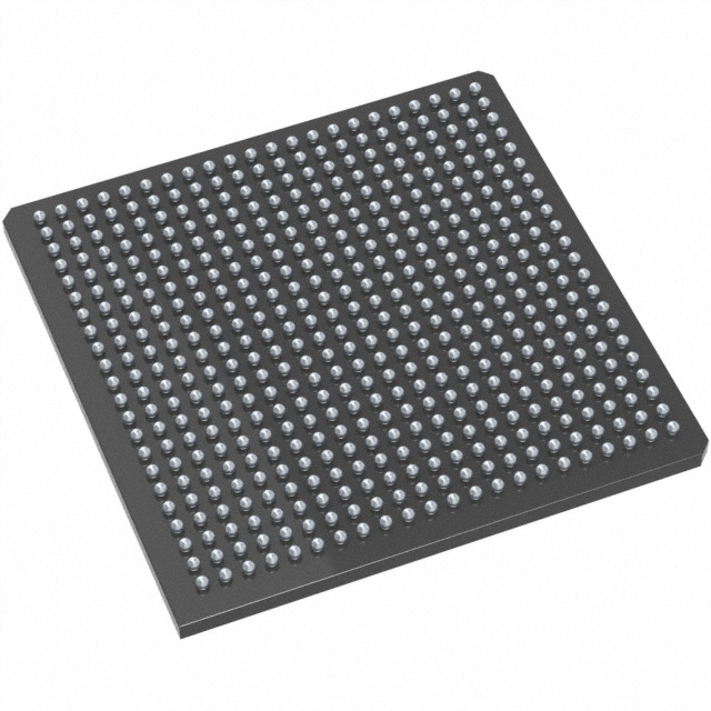
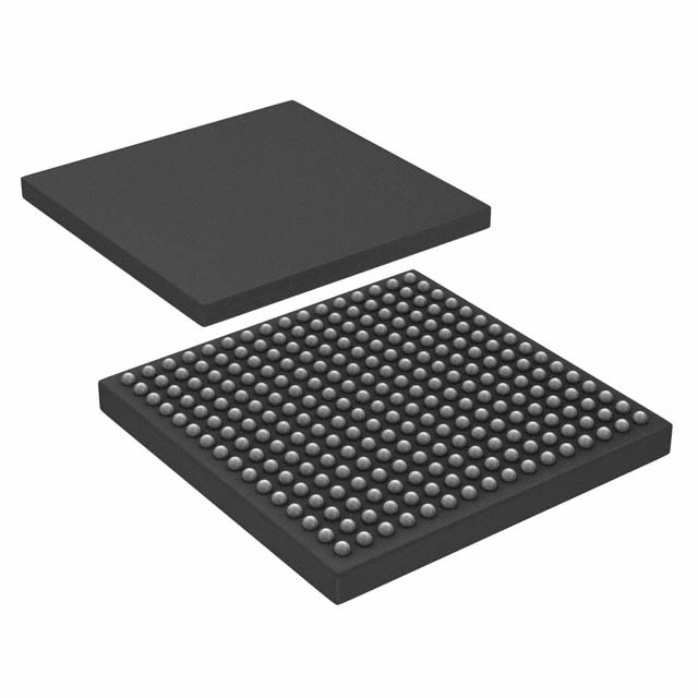
A54SX72A-FGG484M
| Part Description |
SX-A Field Programmable Gate Array (FPGA) IC 360 484-BGA |
|---|---|
| Quantity | 31 Available (as of June 14, 2026) |
| Product Category | Field Programmable Gate Array (FPGA) |
|---|---|
| Manufacturer | Microchip Technology |
| Manufacturing Status | Active |
| Manufacturer Standard Lead Time | 20 Weeks |
| Datasheet |
Specifications & Environmental
| Device Package | 484-FPBGA (27X27) | Grade | Military | Operating Temperature | -55°C – 125°C | ||
|---|---|---|---|---|---|---|---|
| Package / Case | 484-BGA | Number of I/O | 360 | Voltage | 2.25 V - 5.25 V | ||
| Mounting Method | Surface Mount | RoHS Compliance | ROHS3 Compliant | REACH Compliance | REACH Unaffected | ||
| Moisture Sensitivity Level | 3 (168 Hours) | Number of LABs/CLBs | 6036 | Number of Logic Elements/Cells | 6036 | ||
| Number of Gates | 108000 | ECCN | 3A001A2C | HTS Code | 8542.39.0001 | ||
| Qualification | N/A |
Overview of A54SX72A-FGG484M – SX-A Field Programmable Gate Array (FPGA) IC 360 484-BGA
The A54SX72A-FGG484M is a nonvolatile SX-A family FPGA providing 108,000 system gates and 6,036 logic elements in a 484-ball fine-pitch BGA. Designed for military-grade and high-reliability systems, this device combines high gate density, up to 360 user-programmable I/Os and deterministic timing features for demanding embedded and interface applications.
Key value propositions include single-chip nonvolatile configuration, support for mixed-voltage I/O, and operation across a wide supply and temperature range—enabling deployment in harsh environments where reliability and configurability matter.
Key Features
- Core Performance — System performance up to 250 MHz and internal performance up to 350 MHz, providing headroom for timing-critical logic.
- Logic Capacity — 108,000 available system gates and 6,036 logic elements with up to 2,012 dedicated flip-flops for complex logic implementation.
- I/O and Interface Flexibility — Up to 360 user-programmable I/Os; configurable I/O support for 3.3 V/5 V PCI, 5 V TTL, 3.3 V LVTTL and 2.5 V LVCMOS2 standards, with 5 V input tolerance and 5 V drive strength.
- Power and Voltage — Wide supply voltage support from 2.25 V to 5.25 V and power-up/power-down friendly operation with no sequencing required for supply voltages.
- Package and Mounting — 484-ball fine-pitch BGA package (484-FPBGA (27×27)), surface-mount mounting type suited for compact board designs.
- Temperature and Grade — Military grade device with an operating temperature range of −55 °C to 125 °C for demanding environmental conditions.
- System Reliability & Test — Boundary-scan testing compliant with IEEE 1149.1 (JTAG) and in-system diagnostic and verification capability using Silicon Explorer II.
- Security — Actel Secure Programming Technology with FuseLock™ to protect design IP against reverse engineering.
- PCI Compatibility — 66 MHz PCI compliant for integration with PCI-based interfaces.
- On-chip Memory — No embedded RAM on-chip (Total RAM bits: 0), enabling predictable resource allocation for logic and flip-flop usage.
Typical Applications
- Military and Aerospace Systems — Military-grade temperature range and packaging make the device suitable for high-reliability embedded control and interface functions in harsh environments.
- PCI-Based Interface and Peripheral Control — 66 MHz PCI compliance and extensive, configurable I/O support enable use as a bridge or controller for PCI peripheral subsystems.
- High-Reliability Embedded Logic — High gate count and deterministic timing support complex custom logic, signal processing control, and mission-critical state machines.
Unique Advantages
- High Gate Density: 108,000 system gates and 6,036 logic elements provide significant integration density to consolidate logic and reduce BOM.
- Flexible I/O Voltage Support: Configurable I/O standards and 5 V tolerance/drive capability simplify interfacing to legacy and mixed-voltage peripherals.
- Nonvolatile Single-Chip Configuration: Eliminates the need for external configuration memory, simplifying system design and improving boot determinism.
- Designed for Harsh Environments: Military grade rating and −55 °C to 125 °C operation support deployments where temperature extremes and reliability are critical.
- Security and Testability: FuseLock secure programming plus IEEE-1149.1 boundary-scan and in-system diagnostics improve IP protection and production test coverage.
- Deterministic Timing and Diagnostics: User-controllable timing and Silicon Explorer II capability help validate and debug designs in-system.
Why Choose A54SX72A-FGG484M?
The A54SX72A-FGG484M positions itself as a high-density, nonvolatile FPGA option for designs that require robust operation in demanding environments. With a large logic capacity, extensive I/O, mixed-voltage support and military-grade temperature performance, it suits customers building high-reliability embedded systems, PCI-interfacing logic and mission-critical control applications.
Selected for applications where on-board nonvolatile configuration, design security and deterministic behavior are priorities, this FPGA provides a balance of integration, flexibility and reliability backed by the SX-A family feature set.
Request a quote or submit a product inquiry to receive pricing, availability and technical support for the A54SX72A-FGG484M.


Date Founded: 1989
Headquarters: Chandler, Arizona, USA
Employees: 22,000+
Revenue: $8.349 Billion
Certifications and Memberships: ISO9001:2015, IATF16949:2016, AS 9100D


