
AGL250V5-CSG196I
| Part Description |
IGLOO Field Programmable Gate Array (FPGA) IC 143 36864 6144 196-TFBGA, CSBGA |
|---|---|
| Quantity | 721 Available (as of June 18, 2026) |
| Product Category | Field Programmable Gate Array (FPGA) |
|---|---|
| Manufacturer | Microchip Technology |
| Manufacturing Status | Active |
| Manufacturer Standard Lead Time | 8 Weeks |
| Datasheet |
Specifications & Environmental
| Device Package | 196-CSP (8x8) | Grade | Industrial | Operating Temperature | -40°C – 85°C | ||
|---|---|---|---|---|---|---|---|
| Package / Case | 196-TFBGA, CSBGA | Number of I/O | 143 | Voltage | 1.425 V - 1.575 V | ||
| Mounting Method | Surface Mount | RoHS Compliance | ROHS3 Compliant | REACH Compliance | REACH Unaffected | ||
| Moisture Sensitivity Level | 3 (168 Hours) | Number of LABs/CLBs | 6144 | Number of Logic Elements/Cells | 6144 | ||
| Number of Gates | 250000 | ECCN | 3A991D | HTS Code | 8542.39.0001 | ||
| Qualification | N/A | Total RAM Bits | 36864 |
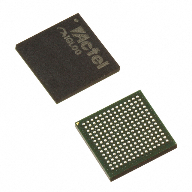
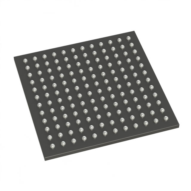
Overview of AGL250V5-CSG196I – IGLOO FPGA, 143 I/Os, 6,144 Logic Elements, 196-TFBGA
The AGL250V5-CSG196I is a Microchip Technology IGLOO flash FPGA in a compact 196‑TFBGA (CSBGA) package. It combines reprogrammable flash-based FPGA fabric with on-chip SRAM and advanced I/O support to address low-power, space-constrained system designs.
Built for industrial-temperature operation and surface-mount assembly, this device is optimized for applications that require instant-on behavior, low standby power, and a mix of high-speed and mixed-voltage I/O capabilities.
Key Features
- Programmable Logic: 6,144 logic elements (cells) providing configurable logic capacity for glue logic, protocol handling, and custom control functions.
- Embedded Memory: Approximately 36.9 kbits of on-chip RAM (36,864 total RAM bits) for buffering, small data tables, and user registers.
- System Gates: Approximately 250,000 system gates for implementing medium-density FPGA designs.
- I/O Density and Standards: 143 I/O pins with support for high-speed DDR (700 Mbps) and LVDS-capable interfaces (AGL250 and above), and mixed-voltage operation across 1.2V, 1.5V, 1.8V, 2.5V and 3.3V domains as described for the IGLOO series.
- Low-Power Modes: Flash*Freeze ultra-low-power mode (as low as 5 μW) and Low Power Active (static idle) capability, enabling minimal standby consumption while retaining FPGA content and operational control.
- Flash-Based Nonvolatile Storage: Reprogrammable flash fabric that retains configuration when powered off and supports instant-on behavior; series devices include on-chip FlashROM storage.
- Clock Conditioning and PLL: Integrated clock conditioning circuitry in the IGLOO family, including CCC blocks and at least one PLL block for clock multiply/divide and phase adjustments (series feature).
- Power and Temperature: Core supply range 1.425 V to 1.575 V and industrial operating temperature range −40 °C to 85 °C.
- Package and Mounting: 196‑TFBGA (CSBGA) package, supplier package 196‑CSP (8×8), surface-mount for compact board-level integration.
- Environmental Compliance: RoHS compliant.
Typical Applications
- Power-Managed Embedded Systems: Use the Flash*Freeze and Low Power Active modes to implement system-level power management and instant-on control without high standby current.
- High-Speed I/O Bridging: Implement DDR and LVDS-capable interfaces and mixed-voltage I/O banks for protocol translation and high-speed interface logic.
- Compact Board-Level FPGA: The 196‑TFBGA package and surface-mount form factor suit space-constrained designs requiring reprogrammable logic and moderate I/O counts.
- Industrial Control and Monitoring: Industrial-grade temperature range and deterministic reprogrammable logic make this device suitable for control, sequencing, and interface tasks in industrial equipment.
Unique Advantages
- Low Standby Power: Flash*Freeze and Low Power Active modes enable extremely low-power retention (down to 5 μW), reducing system power budgets during idle periods.
- Nonvolatile Reprogrammability: Flash-based configuration retains the programmed design when powered off, enabling instant-on behavior and field reprogramming.
- Mixed-Voltage I/O Flexibility: Support for multiple I/O voltage domains and high-speed signaling lets you interface with a wide range of peripherals without external level-shifting.
- Industrial Temperature Rating: −40 °C to 85 °C operation aligns with industrial deployment requirements for reliable field use.
- Compact BGA Footprint: 196-ball BGA package provides a high-density, surface-mount solution for compact PCB layouts while preserving abundant I/O.
- Integrated Clocking Resources: On-device clock conditioning and PLL resources simplify system clock generation and timing management for complex logic designs.
Why Choose AGL250V5-CSG196I?
The AGL250V5-CSG196I brings together reprogrammable flash FPGA fabric, embedded SRAM, high-speed mixed-voltage I/O, and industry-grade thermal performance in a compact 196‑TFBGA package. Its low-power modes and nonvolatile configuration make it a strong fit for designs that require instant-on capability and minimized standby consumption while retaining flexibility for iterative development and field updates.
This device suits engineers building mid-density logic, interface bridging, and industrial control solutions that demand reliable operation across −40 °C to 85 °C, flexible I/O standards, and a small PCB footprint backed by Microchip’s IGLOO family architecture.
Request a quote or submit a quotation request to evaluate availability and pricing for the AGL250V5-CSG196I for your next design.


Date Founded: 1989
Headquarters: Chandler, Arizona, USA
Employees: 22,000+
Revenue: $8.349 Billion
Certifications and Memberships: ISO9001:2015, IATF16949:2016, AS 9100D


