
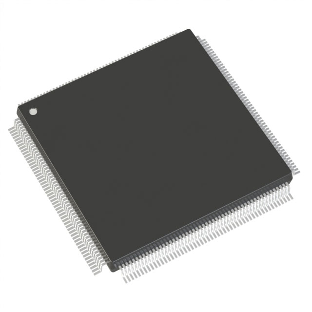
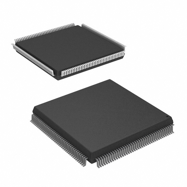
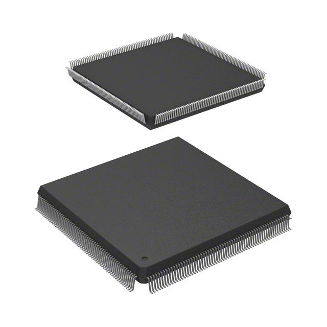
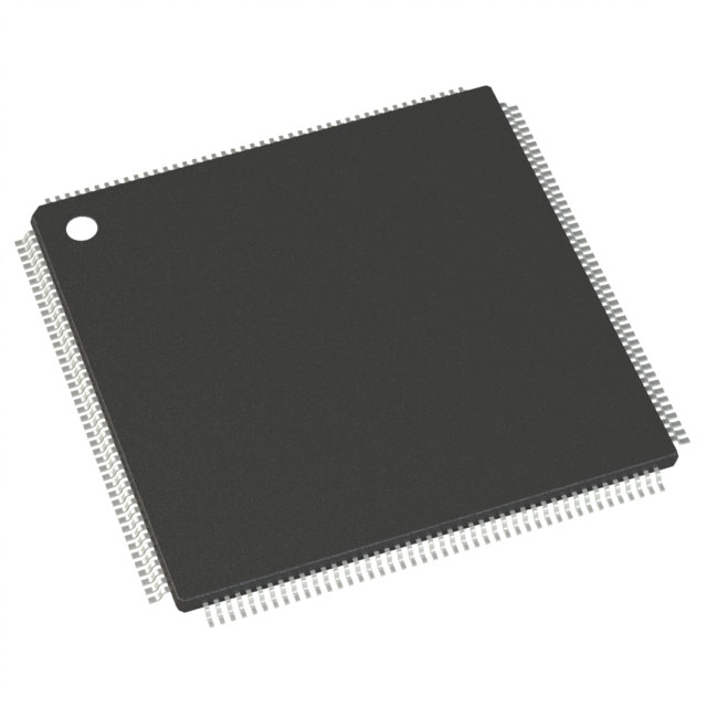
AT40K20AL-1FQC
| Part Description |
AT40KAL Field Programmable Gate Array (FPGA) IC 256 8192 1024 304-BFQFP |
|---|---|
| Quantity | 686 Available (as of June 15, 2026) |

| Product Category | Field Programmable Gate Array (FPGA) |
|---|---|
| Manufacturer | Microchip Technology |
| Manufacturing Status | Obsolete |
| Manufacturer Standard Lead Time | Contact Us |
| Datasheet |
Specifications & Environmental
| Device Package | 304-PQFP (40x40) | Grade | Commercial | Operating Temperature | 0°C – 70°C | ||
|---|---|---|---|---|---|---|---|
| Package / Case | 304-BFQFP | Number of I/O | 256 | Voltage | 3 V - 3.6 V | ||
| Mounting Method | Surface Mount | RoHS Compliance | RoHS non-compliant | REACH Compliance | REACH Unaffected | ||
| Moisture Sensitivity Level | 3 (168 Hours) | Number of LABs/CLBs | 1024 | Number of Logic Elements/Cells | 1024 | ||
| Number of Gates | 30000 | ECCN | 3A991D | HTS Code | 8542.39.0001 | ||
| Qualification | N/A | Total RAM Bits | 8192 |
Overview of AT40K20AL-1FQC – AT40KAL Field Programmable Gate Array (FPGA) IC 256 8192 1024 304-BFQFP
The AT40K20AL-1FQC is an SRAM-based Field Programmable Gate Array from Microchip Technology’s AT40KAL family, offering a mid-density logic resource for commercial embedded designs. This device combines 1,024 logic elements, approximately 8,192 bits of on-chip RAM, and up to 256 I/O pins in a 304-pin PQFP surface-mount package to address computation‑intensive and I/O‑dense applications.
Designed for reconfigurable and high-performance tasks, the device supports features from the AT40KAL series such as fast distributed SRAM, dynamic partial reconfiguration capability, and system speeds up to 100 MHz, making it suitable for DSP acceleration, protocol bridging and other adaptive logic roles in commercial products.
Key Features
- Core logic: 1,024 logic elements providing approximately 30,000 usable gates for mid-range FPGA implementations.
- Embedded memory (FreeRAM): Approximately 8,192 bits of distributed SRAM with 10 ns access times for flexible single/dual-port or synchronous/asynchronous memory functions.
- I/O capability: Up to 256 I/O pins allowing high-density interfacing and programmable output drive options.
- Clocking and timing: Series features include support for multiple global clocks and timing options with system speeds specified up to 100 MHz.
- Power and voltage: Supply voltage range 3.0 V to 3.6 V with 5 V I/O tolerance noted in the series documentation.
- Package and mounting: 304-pin BFQFP/PQFP (40 × 40 mm) surface-mount package suitable for standard PCB assembly processes.
- Commercial temperature grade: Specified operating temperature range 0 °C to 70 °C for commercial applications.
- RoHS compliant: Complies with RoHS environmental requirements.
Typical Applications
- DSP acceleration and coprocessor tasks: Implement adaptive FIR filters, FFTs, convolvers and other arithmetic-heavy functions to offload processors and improve system throughput.
- Video and multimedia processing: Use the device’s fast array multipliers and distributed SRAM for tasks such as compression, decompression and real‑time data manipulation.
- High-density I/O bridging: Integrate multiple interfaces or act as protocol bridges where up to 256 I/Os and programmable drive are required.
- Reconfigurable logic and adaptive systems: Leverage dynamic partial/full reconfiguration capabilities to enable in‑system updates and runtime adaptability.
Unique Advantages
- Balanced mid-range capacity: Combines 1,024 logic elements with roughly 30k gates to target designs requiring moderate gate counts without overprovisioning.
- Fast on-chip memory: Distributed 10 ns SRAM (FreeRAM) enables low-latency storage for FIFOs, scratchpads and coefficient tables while preserving logic resources.
- High I/O density: Up to 256 I/Os in a 304-pin package simplifies board-level routing for peripheral-rich systems.
- Flexible clocking: Series-level support for multiple global clocks and programmable edges helps manage timing and power domains in complex designs.
- Industry tool compatibility: The AT40KAL family is designed for use with standard FPGA synthesis and verification tool flows (as documented for the series), easing integration into existing design environments.
- RoHS compliant commercial solution: Meets environmental compliance needs for mainstream commercial products with an operating temperature of 0 °C to 70 °C.
Why Choose AT40K20AL-1FQC?
The AT40K20AL-1FQC positions itself as a practical choice for developers who need a reconfigurable, mid-density FPGA with a strong mix of logic, memory and I/O resources. Its combination of approximately 1,024 logic elements, 8,192 bits of embedded RAM, and support for system speeds up to 100 MHz provides a capable platform for signal processing, interface logic and adaptive systems in commercial applications.
Engineers and product teams seeking a commercially graded FPGA with in‑system reconfiguration capabilities, ample on‑chip memory and high I/O count will find the AT40K20AL-1FQC an effective building block for scalable, performance-oriented designs backed by the AT40KAL series feature set.
Request a quote or submit a product inquiry to receive pricing and availability for the AT40K20AL-1FQC and to discuss how this FPGA can fit your next design.


Date Founded: 1989
Headquarters: Chandler, Arizona, USA
Employees: 22,000+
Revenue: $8.349 Billion
Certifications and Memberships: ISO9001:2015, IATF16949:2016, AS 9100D


