
M1AGL250V5-VQ100
| Part Description |
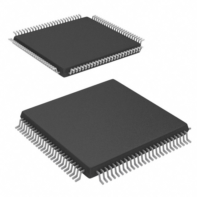
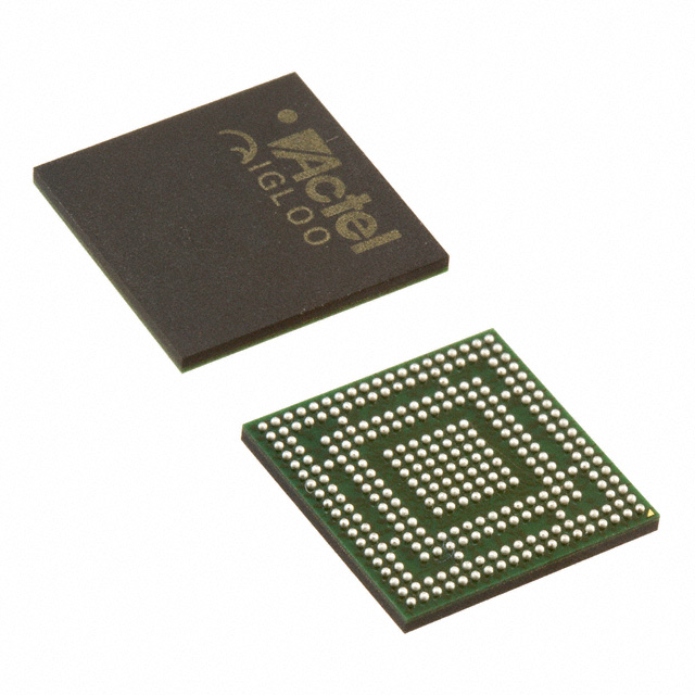
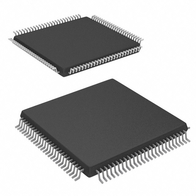
IGLOO Field Programmable Gate Array (FPGA) IC 68 36864 6144 100-TQFP |
|---|---|
| Quantity | 68 Available (as of October 7, 2026) |

| Product Category | Field Programmable Gate Array (FPGA) |
|---|---|
| Manufacturer | Microchip Technology |
| Manufacturing Status | Active |
| Manufacturer Standard Lead Time | 12 Weeks |
| Datasheet |
Specifications & Environmental
| Device Package | 100-VQFP (14x14) | Grade | Commercial | Operating Temperature | 0°C – 70°C | ||
|---|---|---|---|---|---|---|---|
| Package / Case | 100-TQFP | Number of I/O | 68 | Voltage | 1.425 V - 1.575 V | ||
| Mounting Method | Surface Mount | RoHS Compliance | RoHS non-compliant | REACH Compliance | REACH Unaffected | ||
| Moisture Sensitivity Level | 3 (168 Hours) | Number of LABs/CLBs | 6144 | Number of Logic Elements/Cells | 6144 | ||
| Number of Gates | 250000 | ECCN | 3A991D | HTS Code | 8542.39.0001 | ||
| Qualification | N/A | Total RAM Bits | 36864 |
Overview of M1AGL250V5-VQ100 – IGLOO Field Programmable Gate Array (FPGA) IC, 68 I/Os, 36,864-bit RAM, 6,144 logic elements, 100-TQFP
The M1AGL250V5-VQ100 is an IGLOO family flash FPGA optimized for low-power, single-chip embedded designs. Based on the IGLOO low-power flash FPGA architecture, it combines reprogrammable nonvolatile configuration, a compact 100‑TQFP package, and hardware resources suited for control, interface, and signal-processing tasks in commercial-grade systems.
This device is targeted at applications that require ultra-low-power standby and rapid wake-up, mixed-voltage I/O flexibility, and on-chip logic and RAM for moderate-density designs. It is specified for commercial operation from 0 °C to 70 °C and is RoHS compliant.
Key Features
- Logic Capacity — 6,144 logic elements (approximately 250,000 system gates) provide programmable fabric for control, glue logic, and custom processing.
- Embedded Memory — Total on-chip RAM of 36,864 bits plus 1 kbit of on-chip reprogrammable FlashROM for configuration storage and small data retention.
- Low-Power Modes — Flash*Freeze ultra-low-power retention mode consumes as little as 5 μW; Low Power Active (static idle) operation available from 12 μW, enabling minimal power draw while remaining functional.
- Power Supply — Device voltage supply specified at 1.425 V to 1.575 V to support core operation within defined limits.
- I/O and Interfaces — 68 user I/Os; AGL250-class devices support high-speed DDR (up to 700 Mbps) and LVDS-capable I/Os and mixed-voltage operation across common I/O standards.
- Clocking and Timing — Six clock conditioning (CCC) blocks with one integrated PLL for on-chip clock conditioning, phase shift, and multiply/divide functionality.
- Package and Mounting — 100‑TQFP package (supplier device package: 100‑VQFP, 14×14 mm); surface-mount mounting type for compact board-level integration.
- Security & Programming — Reprogrammable flash configuration supports instant-on behavior; ARM-enabled ordering numbers (M1AGL prefix) do not support on-chip AES decryption per family documentation.
- Commercial Grade & Compliance — Specified for 0 °C to 70 °C operation and RoHS compliant for worldwide commercial applications.
Typical Applications
- Low-power embedded controllers — Use Flash*Freeze and Low Power Active modes to implement controllers that monitor system inputs while minimizing standby current.
- Sensor aggregation and interface bridging — Combine multiple sensor inputs, perform preprocessing, and present consolidated interfaces using available logic and RAM.
- High-speed I/O and protocol conversion — Leverage DDR-capable and LVDS-capable I/Os for high-throughput signaling and protocol translation in communication or data-acquisition fronts.
- Soft-processor implementations — Implement Cortex‑M1 soft processor cores within the FPGA fabric for embedded control and deterministic firmware tasks (M1 IGLOO support noted in family documentation).
Unique Advantages
- Ultra-low standby power: Flash*Freeze retention at micro-watt levels enables designs with long idle periods and immediate wake-up capability while retaining SRAM/register state.
- Single-chip, nonvolatile configuration: On-chip flash removes the need for external configuration memory and enables instant-on behavior for faster system startup.
- Mixed-voltage, high-speed I/O: AGL250-class I/O capabilities support a wide range of signaling standards and high-speed interfaces to simplify board-level design.
- Compact surface-mount package: 100‑TQFP (14×14 mm) package balances I/O count and board footprint for space-constrained applications.
- Integrated clocking resources: Multiple CCC blocks and an integrated PLL enable flexible clock generation and distribution without external clock-conditioning components.
- Commercial-grade reliability: Designed for 0 °C to 70 °C operation and RoHS compliance for standard commercial deployable products.
Why Choose M1AGL250V5-VQ100?
The M1AGL250V5-VQ100 delivers a balanced combination of low-power operation, reprogrammable nonvolatile configuration, and moderate FPGA resources ideal for commercial embedded designs. With 6,144 logic elements, approximately 36,864 bits of embedded RAM, flexible high-speed I/Os, and integrated clock-conditioning blocks, it supports control, interfacing, and preprocessing tasks without large external component counts.
This part is well suited for designers who need a compact, surface-mount FPGA with instant-on capability and ultra-low standby power, and who prefer the predictability of flash-based configuration for commercial products. Its family-level features, such as Flash*Freeze and CCC/PLL resources, provide system-level power and clock management advantages while keeping BOM complexity low.
Request a quote or submit an inquiry to obtain pricing and availability for the M1AGL250V5-VQ100.























Date Founded: 1989
Headquarters: Chandler, Arizona, USA
Employees: 22,000+
Revenue: $8.349 Billion
Certifications and Memberships: ISO9001:2015, IATF16949:2016, AS 9100D




