
M2GL010TS-1FGG484T2
| Part Description |
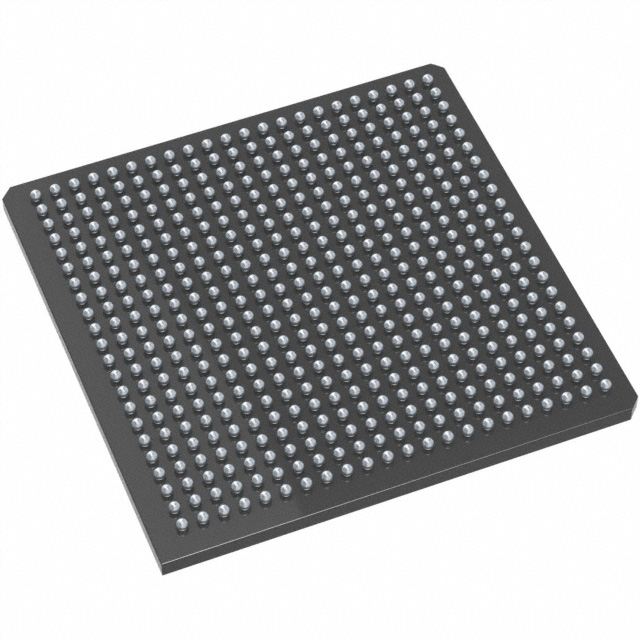
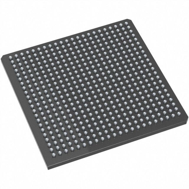
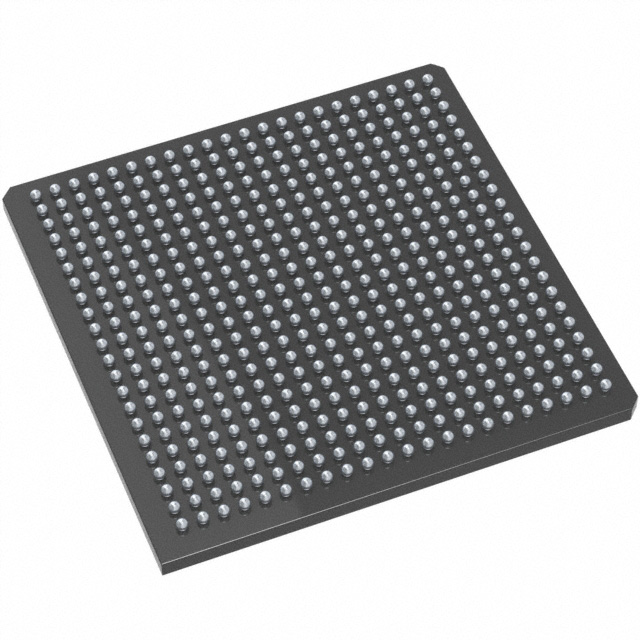
IGLOO2 Field Programmable Gate Array (FPGA) IC 233 933888 12084 484-BGA |
|---|---|
| Quantity | 73 Available (as of October 8, 2026) |

| Product Category | Field Programmable Gate Array (FPGA) |
|---|---|
| Manufacturer | Microchip Technology |
| Manufacturing Status | Active |
| Manufacturer Standard Lead Time | 16 Weeks |
| Datasheet |
Specifications & Environmental
| Device Package | 484-FPBGA (23x23) | Grade | Automotive | Operating Temperature | -40°C – 125°C | ||
|---|---|---|---|---|---|---|---|
| Package / Case | 484-BGA | Number of I/O | 233 | Voltage | 1.14 V - 2.625 V | ||
| Mounting Method | Surface Mount | RoHS Compliance | ROHS3 Compliant | REACH Compliance | REACH Unaffected | ||
| Moisture Sensitivity Level | 3 (168 Hours) | Number of LABs/CLBs | 12084 | Number of Logic Elements/Cells | 12084 | ||
| Number of Gates | N/A | ECCN | 5A002A1 | HTS Code | 8542.39.0001 | ||
| Qualification | AEC-Q100 | Total RAM Bits | 933888 |
Overview of M2GL010TS-1FGG484T2 – IGLOO2 FPGA, 12084 logic elements, 484-BGA
The M2GL010TS-1FGG484T2 is an IGLOO2 family Field Programmable Gate Array (FPGA) IC from Microchip Technology. It leverages fourth-generation flash-based FPGA fabric to deliver low-power, secure, and reliable programmable logic suitable for embedded and automotive applications. This device targets designs requiring substantial on-chip logic, significant I/O connectivity, and robust operating ranges for harsh environments.
Key Features
- Core Logic Approximately 12,084 logic elements implemented in IGLOO2’s 4-input LUT fabric with carry chains for efficient logic implementation and performance.
- On‑Chip Memory Approximately 0.93 Mbits (933,888 bits) of total RAM. IGLOO2 family descriptions include multiple embedded memory options such as dual-port 18 Kbit SRAM blocks and micro SRAM arrays.
- DSP and Math Resources Family-level DSP resources include fast mathblocks for signed/unsigned multiplications and wide accumulators suitable for signal processing tasks.
- High‑Speed Serial & Comms IGLOO2 family features high-speed serial capabilities (for example, native SERDES lanes and support for PCIe and 10 Gbps PHY interfaces) to enable high-bandwidth link implementations.
- High‑Speed Memory Interfaces Family controllers support DDRx memory types (LPDDR/DDR2/DDR3) with synchronous operation and memory command/data ordering features for optimized throughput.
- I/O and Voltage 233 user I/Os with multi-standard support; device supply range 1.14 V to 2.625 V and a documented 1.2 V core voltage in the IGLOO2 architecture.
- Package & Mounting 484-BGA package (supplier device package: 484-FPBGA, 23 × 23) designed for surface-mount assembly.
- Automotive Qualification Grade: Automotive with AEC‑Q100 qualification; operating temperature range −40 °C to 125 °C.
- Security & Reliability (family‑level) IGLOO2 family includes design and data security features such as encrypted bitstream loading, device certificate support, anti-tamper mechanisms, and optional cryptographic services described at the family level.
- RoHS Compliance Device is RoHS compliant.
Typical Applications
- Automotive electronics AEC‑Q100 qualification and −40 °C to 125 °C operation make this device suitable for in-vehicle systems that need programmable logic with robust thermal margins.
- High-speed communications Use where SERDES lanes, PCIe endpoints or 10 Gbps PHY interfaces are required for networking, backbone, or data transport functions.
- Embedded memory controllers and buffering On-chip RAM and IGLOO2 DDRx controller features support designs that require local buffering, DMA offload, or memory-bridge functions.
- Signal processing and sensor aggregation DSP mathblocks and abundant logic elements support digital filtering, aggregation, and pre-processing of sensor data in embedded systems.
Unique Advantages
- Automotive‑grade qualification: AEC‑Q100 qualification and a wide operating temperature range provide confidence for vehicle-level deployments.
- Balanced integration of logic and memory: 12,084 logic elements coupled with approximately 0.93 Mbits of on-chip RAM enable compact, self-contained designs with reduced external memory dependence.
- High I/O count and multi‑standard support: 233 I/Os and multi-standard signaling capability simplify interfacing to diverse peripherals and memory types.
- Flexible power domain support: Broad supply range (1.14 V to 2.625 V) and 1.2 V core architecture accommodate a variety of system power architectures.
- Surface-mount 484‑BGA packaging: High-pin-count ball grid package supports dense designs while maintaining standard surface-mount assembly compatibility.
- Family-level communications and security features: IGLOO2 architecture provides high-speed serial interfaces, DDR controllers, and security primitives to address complex system requirements without multiple discrete components.
Why Choose M2GL010TS-1FGG484T2?
The M2GL010TS-1FGG484T2 delivers a practical balance of programmable logic capacity, embedded memory, and I/O density within the IGLOO2 flash‑based FPGA architecture. Its automotive qualification, robust temperature range, and family-level high-speed and security features make it a compelling choice for engineers building reliable, integrated systems that must meet stringent environmental and functional requirements.
Design teams that need on-chip DSP capability, flexible memory interfacing, and a high number of user I/Os will find this device well suited to scalable embedded and automotive applications while benefiting from the IGLOO2 family’s architectural features.
Request a quote or submit a pricing inquiry to receive availability and lead-time information for the M2GL010TS-1FGG484T2.























Date Founded: 1989
Headquarters: Chandler, Arizona, USA
Employees: 22,000+
Revenue: $8.349 Billion
Certifications and Memberships: ISO9001:2015, IATF16949:2016, AS 9100D




