
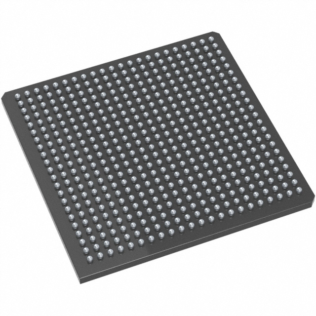
M2GL025-1FGG484
| Part Description |
IGLOO2 Field Programmable Gate Array (FPGA) IC 267 1130496 27696 484-BGA |
|---|---|
| Quantity | 320 Available (as of October 7, 2026) |
| Product Category | Field Programmable Gate Array (FPGA) |
|---|---|
| Manufacturer | Microchip Technology |
| Manufacturing Status | Active |
| Manufacturer Standard Lead Time | 10 Weeks |
| Datasheet |
Specifications & Environmental
| Device Package | 484-FPBGA (23x23) | Grade | Commercial | Operating Temperature | 0°C – 85°C | ||
|---|---|---|---|---|---|---|---|
| Package / Case | 484-BGA | Number of I/O | 267 | Voltage | 1.14 V - 2.625 V | ||
| Mounting Method | Surface Mount | RoHS Compliance | ROHS3 Compliant | REACH Compliance | REACH Unaffected | ||
| Moisture Sensitivity Level | 3 (168 Hours) | Number of LABs/CLBs | 27696 | Number of Logic Elements/Cells | 27696 | ||
| Number of Gates | N/A | ECCN | 3A991D | HTS Code | 8542.39.0001 | ||
| Qualification | N/A | Total RAM Bits | 1130496 |
Overview of M2GL025-1FGG484 – IGLOO2 Field Programmable Gate Array (FPGA) IC 267 1130496 27696 484-BGA
The M2GL025-1FGG484 is a Microchip Technology IGLOO2 family FPGA featuring flash-based programmable logic and high-performance communications interfaces. This device combines a 4-input LUT fabric with built-in memory and DSP resources, making it suitable for designs that require dense logic, embedded memory, and advanced serial or memory interfaces.
Designed for commercial applications, the device targets implementations that need a balance of integration, power efficiency, and flexible I/O and memory interfacing.
Key Features
- Logic Capacity Approximately 27,696 logic elements, providing substantial fabric resources for complex designs.
- Embedded Memory Approximately 1.13 Mbits of total on-chip RAM (1,130,496 bits) for buffering and data storage.
- I/O Density 267 user I/Os to support multiple peripheral interfaces and board-level connections.
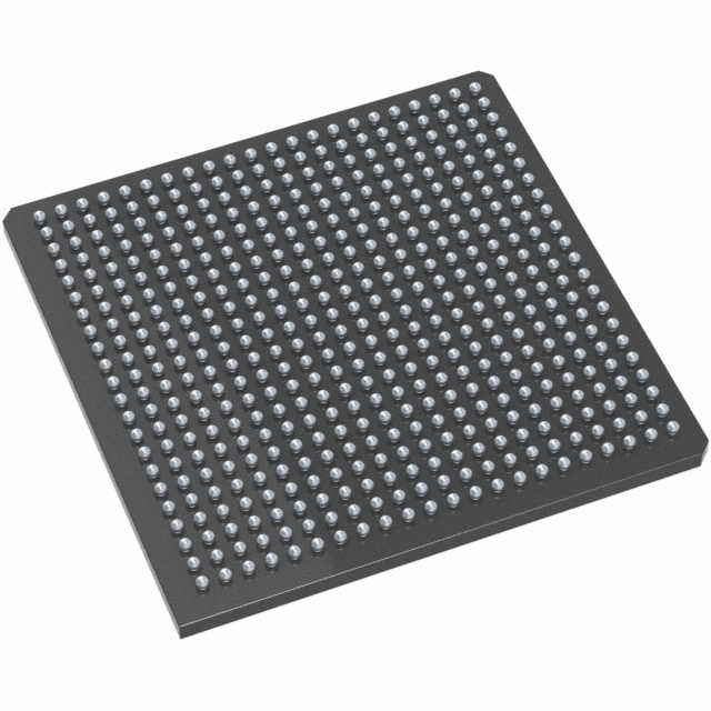
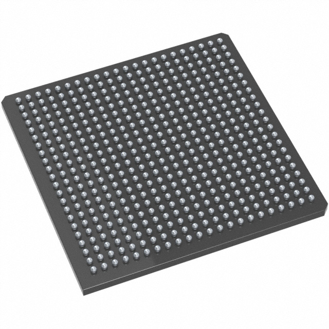
- Package & Mounting 484-ball BGA package (484-FPBGA, 23 × 23) in a surface-mount form factor for compact board integration.
- Supply Voltage Wide supply support from 1.14 V to 2.625 V to accommodate core and I/O domain requirements.
- Operating Range Commercial temperature grade with an operating temperature range of 0 °C to 85 °C.
- Environmental Compliance RoHS compliant.
- Flash-Based FPGA Architecture (IGLOO2 family) Fourth-generation flash-based fabric with 4-input LUTs and carry chains for efficient implementation of combinational and arithmetic logic.
- High-Performance DSP & Memory Subsystems (IGLOO2 family) Family-level capabilities include up to 240 mathblocks for multiply/accumulate operations, 64 KB of embedded SRAM (eSRAM), and up to 512 KB of embedded nonvolatile memory (eNVM).
- High-Speed Serial and Memory Interfaces (IGLOO2 family) Family features include up to 16 SERDES lanes, PCIe endpoint cores, and up to two DDRx controllers supporting DDR2/DDR3/LPDDR modes (family-level specifications).
Typical Applications
- High-Speed Communication Modules Use the IGLOO2 family’s SERDES lanes and PCIe support to implement serial links and protocol bridging.
- Memory Interface Controllers Leverage the built-in DDRx memory controller capabilities to connect external DDR2/DDR3 memory for buffering and high-throughput data paths.
- DSP and Signal Processing Employ on-chip mathblocks and embedded RAM for real-time signal processing, filtering, and accumulation tasks.
- Embedded System Glue Logic Use the device’s abundant I/Os and logic elements to integrate peripherals, implement protocol converters, or centralize control functions on a single chip.
Unique Advantages
- Flash-Based, Reprogrammable Architecture: IGLOO2’s flash-based fabric provides nonvolatile configuration and reprogrammability while supporting deployment in locations where on-chip nonvolatile memory is preferred.
- Integrated Memory and DSP Resources: Combined on-chip RAM (approximately 1.13 Mbits), eSRAM, eNVM, and mathblocks reduce external component needs for buffering and signal processing.
- High I/O Count with Advanced SerDes Support: 267 user I/Os paired with family-level SERDES lanes enable complex board-level interfaces and high-speed serial connectivity.
- Flexible Voltage Domains: Support for 1.14 V to 2.625 V supply ranges accommodates a variety of core and I/O voltage plans.
- Commercial Temperature and RoHS Compliance: Rated for 0 °C to 85 °C operation and RoHS compliant for standard commercial designs.
- Compact BGA Package: 484-ball FPBGA (23 × 23) enables high-density PCB designs while providing the pin count required for complex systems.
Why Choose M2GL025-1FGG484?
The M2GL025-1FGG484 delivers a combination of sizable logic resources, embedded memory capacity, and versatile I/O in a compact 484-BGA package. As part of the IGLOO2 family, it benefits from a flash-based FPGA architecture and family-level features such as DSP mathblocks, embedded SRAM/eNVM, and high-speed serial and memory interfaces—attributes that help reduce external components and streamline system integration.
This device is suited for commercial designs that need integrated memory and DSP capabilities, flexible I/O, and configurable serial/memory connectivity while maintaining reprogrammability and compact board footprint. Its commercial temperature rating and RoHS compliance make it suitable for a broad range of standard embedded applications.
Request a quote or submit a pricing and availability request to learn more about incorporating the M2GL025-1FGG484 into your next design.

























Date Founded: 1989
Headquarters: Chandler, Arizona, USA
Employees: 22,000+
Revenue: $8.349 Billion
Certifications and Memberships: ISO9001:2015, IATF16949:2016, AS 9100D




