
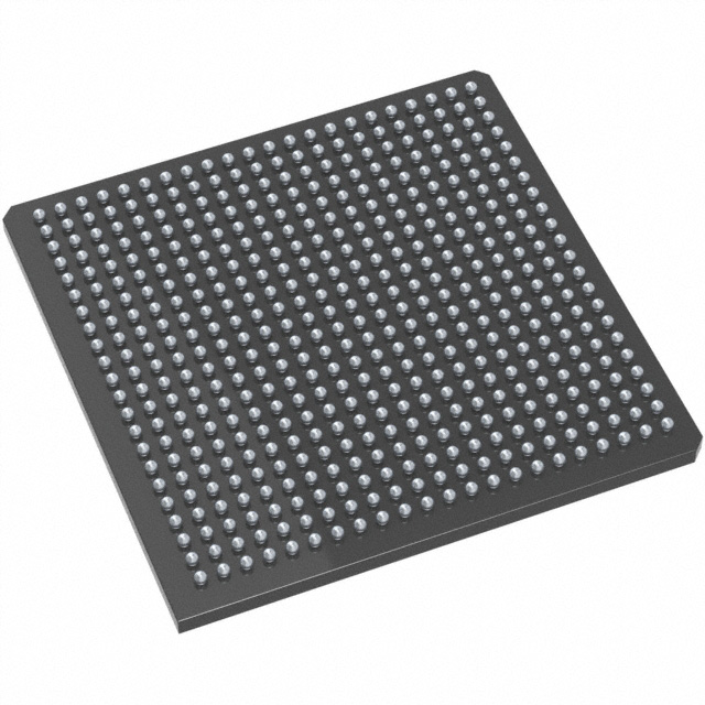
M2GL025-1FGG484I
| Part Description |
IGLOO2 Field Programmable Gate Array (FPGA) IC 267 1130496 27696 484-BGA |
|---|---|
| Quantity | 557 Available (as of June 15, 2026) |

| Product Category | Field Programmable Gate Array (FPGA) |
|---|---|
| Manufacturer | Microchip Technology |
| Manufacturing Status | Active |
| Manufacturer Standard Lead Time | 10 Weeks |
| Datasheet |
Specifications & Environmental
| Device Package | 484-FPBGA (23x23) | Grade | Industrial | Operating Temperature | -40°C – 100°C | ||
|---|---|---|---|---|---|---|---|
| Package / Case | 484-BGA | Number of I/O | 267 | Voltage | 1.14 V - 2.625 V | ||
| Mounting Method | Surface Mount | RoHS Compliance | ROHS3 Compliant | REACH Compliance | REACH Unaffected | ||
| Moisture Sensitivity Level | 3 (168 Hours) | Number of LABs/CLBs | 27696 | Number of Logic Elements/Cells | 27696 | ||
| Number of Gates | N/A | ECCN | 3A991D | HTS Code | 8542.39.0001 | ||
| Qualification | N/A | Total RAM Bits | 1130496 |
Overview of M2GL025-1FGG484I – IGLOO2 FPGA, 27,696 Logic Elements, 267 I/Os
The M2GL025-1FGG484I is a Microchip IGLOO2 field-programmable gate array (FPGA) in a 484-ball BGA package. It combines flash-based FPGA fabric with high-performance communications and memory interfaces suitable for industrial embedded systems and secure applications.
Designed for low-power and reliable operation, this device targets use in high-speed serial communications, memory-intensive designs, DSP acceleration and secure embedded subsystems while offering broad I/O flexibility and an industrial temperature rating.
Key Features
- Logic Capacity — 27,696 logic elements available for implementing combinational and sequential logic.
- Embedded Memory — Approximately 1.13 Mbits of on-chip RAM (total RAM bits: 1,130,496) for data buffering and local storage.
- I/O and Voltage — 267 user I/Os with a voltage supply range of 1.14 V to 2.625 V and support for multiple I/O standards as described in IGLOO2 family documentation.
- High-Speed Interfaces — Family-level support for high-speed serial interfaces (SERDES lanes), PCI Express, and XAUI/XGMII class interfaces as part of the IGLOO2 architecture.
- Memory Controllers — IGLOO2 family supports high-speed DDRx memory controllers (DDR2/DDR3/LPDDR) and flexible DRAM bus width modes for memory-intensive applications.
- DSP and Mathblocks — IGLOO2 architecture includes dedicated mathblocks for DSP tasks and signed/unsigned multipliers and accumulators (family-level capability).
- Clocking Resources — On-chip clocking options in the IGLOO2 family include multiple oscillators and clock conditioning circuits with integrated PLLs for flexible clock management.
- Package & Mounting — 484-FPBGA (23 × 23) surface-mount package for compact board-level integration.
- Industrial Temperature Range — Rated for operation from −40°C to 100°C for deployment in industrial environments.
- RoHS Compliant — Meets RoHS environmental requirements.
Typical Applications
- High-Speed Communications — Implement serial links, PHY interfaces and protocol bridging using the family’s SERDES and PCIe-capable fabrics.
- Memory-Intensive Systems — Use integrated memory resources and DDRx controllers for buffering, frame storage or packet processing in network and edge systems.
- DSP Acceleration — Offload compute-intensive tasks such as filtering, FFTs or real-time signal processing using on-chip mathblocks and local RAM.
- Industrial Control & Automation — Leverage the industrial temperature rating and flexible I/O standards for motor control, sensor aggregation and real-time control logic.
- Secure Embedded Systems — Deploy in applications requiring encrypted bitstreams and device-level security features available in the IGLOO2 family.
Unique Advantages
- Flash-Based Low-Power Fabric: Flash-based IGLOO2 architecture delivers nonvolatile configuration and reduced power compared to volatile PLD technologies.
- High Logic and Memory Density: 27,696 logic elements and approximately 1.13 Mbits of embedded RAM enable complex logic integration and local buffering on a single device.
- Wide I/O Flexibility: 267 I/Os and multi-standard I/O support allow direct interfacing with a broad range of peripherals and memory devices.
- Integrated High-Speed Interfaces: Family-level SERDES, PCIe and XAUI/XGMII capabilities simplify high-bandwidth link implementation without extensive external PHYs.
- Industrial Reliability: Surface-mount 484-FPBGA package and −40°C to 100°C operating range support deployment in rugged industrial environments.
- Security and System Reliability: IGLOO2 family security features (encrypted bitstreams, device certificates and optional cryptographic services) support protected designs and supply-chain assurance.
Why Choose M2GL025-1FGG484I?
The M2GL025-1FGG484I provides a practical balance of logic capacity, embedded memory and extensive I/O in a flash-based IGLOO2 FPGA. Its combination of on-chip RAM, DSP math resources and family-level high-speed interfaces makes it suitable for demanding embedded and communications applications where low power, security and industrial temperature operation are priorities.
Engineers seeking to consolidate functions, reduce external components and deploy secure, field-programmable solutions will find this device aligns with long-term scalability and robust system design goals.
Request a quote or submit an inquiry to receive pricing and availability information for the M2GL025-1FGG484I. Our team will assist with technical details and order support.


Date Founded: 1989
Headquarters: Chandler, Arizona, USA
Employees: 22,000+
Revenue: $8.349 Billion
Certifications and Memberships: ISO9001:2015, IATF16949:2016, AS 9100D


