
M2GL025-1VF400I
| Part Description |
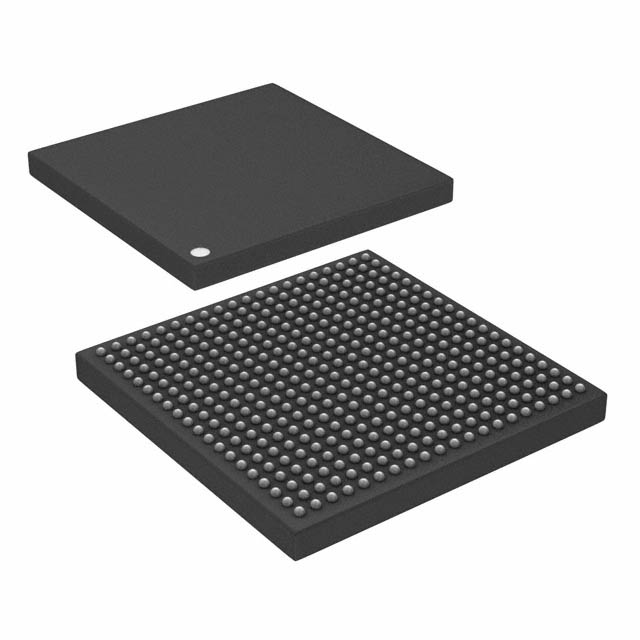
IGLOO2 Field Programmable Gate Array (FPGA) IC 207 1130496 27696 400-LFBGA |
|---|---|
| Quantity | 818 Available (as of June 18, 2026) |
| Product Category | Field Programmable Gate Array (FPGA) |
|---|---|
| Manufacturer | Microchip Technology |
| Manufacturing Status | Active |
| Manufacturer Standard Lead Time | 10 Weeks |
| Datasheet |
Specifications & Environmental
| Device Package | 400-VFBGA (17x17) | Grade | Industrial | Operating Temperature | -40°C – 100°C | ||
|---|---|---|---|---|---|---|---|
| Package / Case | 400-LFBGA | Number of I/O | 207 | Voltage | 1.14 V - 2.625 V | ||
| Mounting Method | Surface Mount | RoHS Compliance | RoHS non-compliant | REACH Compliance | REACH Unaffected | ||
| Moisture Sensitivity Level | 3 (168 Hours) | Number of LABs/CLBs | 27696 | Number of Logic Elements/Cells | 27696 | ||
| Number of Gates | N/A | ECCN | 3A991D | HTS Code | 8542.39.0001 | ||
| Qualification | N/A | Total RAM Bits | 1130496 |
Overview of M2GL025-1VF400I – IGLOO2 Field Programmable Gate Array (FPGA) IC 207 1130496 27696 400-LFBGA
The M2GL025-1VF400I is an IGLOO2-series flash-based FPGA offering a balanced combination of programmable logic, embedded memory, and high-performance communications interfaces. It is built on Microsemi's IGLOO2 architecture and is suited for designs that require low-power operation, integrated memory and DSP resources, and advanced serial and memory interfaces.
Typical use cases for this device include communications and networking modules, DSP and signal-processing subsystems, and systems that need robust on-chip memory and I/O counts within an industrial temperature range.
Key Features
- Logic Capacity Approximately 27,696 logic elements, implemented with a 4-input LUT fabric and carry chains for efficient logic and arithmetic operations.
- Embedded Memory Approximately 1.13 Mbits of on-chip RAM, combined with IGLOO2 family memory options including multiple block SRAM configurations and micro SRAM for flexible data storage.
- DSP Resources IGLOO2 family mathblocks support high-performance signed and unsigned multiplication and wide accumulators for DSP workloads.
- High-Speed Serial Interfaces Family features include up to 16 SERDES lanes and support for PCIe and XAUI/XGMII-style serial interfaces to enable high-throughput communications.
- High-Speed Memory Interfaces IGLOO2 family devices can include up to two DDRx memory controllers supporting DDR2/DDR3 and related modes for external memory connectivity.
- Security and Reliability IGLOO2 family architecture includes encrypted bitstream loading, supply-chain device certificates, and additional security primitives available on premium devices to protect IP and data.
- Package and I/O 400-LFBGA package (supplier device package: 400-VFBGA 17×17) with 207 user I/Os to support dense system interfaces and board-level integration.
- Power and Voltage Operates across a supply range of 1.14 V to 2.625 V, enabling flexibility in system power rails.
- Industrial Temperature Rating Specified for operation from −40 °C to 100 °C, suitable for industrial applications and harsher environments.
- RoHS Compliant & Surface Mount Lead-free, RoHS-compliant device in a surface-mount BGA package for modern assembly processes.
Typical Applications
- High-speed networking and communications Use the device's SERDES lanes and PCIe-capable interfaces to implement PHY/endpoint logic, packet processing, and protocol bridging.
- DSP and signal processing Leverage the IGLOO2 mathblocks and on-chip memory for filters, transforms, and real-time signal-processing kernels.
- Memory interface controllers Employ the on-chip DDRx controller support and embedded memory to build buffering, caching, and high-bandwidth memory subsystems.
- Secure embedded systems Implement encrypted bitstreams and available cryptographic primitives to protect IP and data in security-sensitive designs.
Unique Advantages
- Integrated logic and memory On-chip logic and approximately 1.13 Mbits of embedded RAM reduce external memory dependency and simplify board design.
- Scalable serial and memory interfaces Support for multiple SERDES lanes and DDRx controllers lets designers scale bandwidth without extensive external PHYs.
- Industrial-ready thermal range Rated from −40 °C to 100 °C for deployment in industrial and temperature-challenging environments.
- Flexible I/O and packaging 207 I/Os in a 400-LFBGA package provide a high pin-count solution for complex system connectivity in a compact form factor.
- Security-focused architecture IGLOO2 family features for encrypted bitstreams and device-level protections help secure supply chain and IP integrity.
- RoHS-compliant surface-mount solution Modern assembly compatibility and environmental compliance for commercial production.
Why Choose M2GL025-1VF400I?
The M2GL025-1VF400I brings IGLOO2-family capabilities—flash-based FPGA fabric, substantial embedded memory, DSP resources, and high-speed serial/memory interfaces—into a single 400-LFBGA device rated for industrial temperatures. It is well suited to engineers developing communications, signal-processing, or secure embedded systems that require a combination of on-chip resources and flexible I/O.
Choosing this device provides a compact, industrial-grade programmable logic solution with design flexibility thanks to its logic capacity, embedded RAM, and I/O richness, backed by IGLOO2 family features for low-power operation and enhanced security models.
Request a quote or submit an inquiry to receive pricing, availability, and technical support information for the M2GL025-1VF400I.


Date Founded: 1989
Headquarters: Chandler, Arizona, USA
Employees: 22,000+
Revenue: $8.349 Billion
Certifications and Memberships: ISO9001:2015, IATF16949:2016, AS 9100D


