
M2GL025-1VFG400
| Part Description |
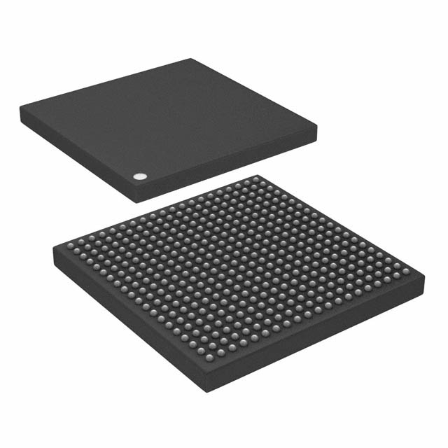
IGLOO2 Field Programmable Gate Array (FPGA) IC 207 1130496 27696 400-LFBGA |
|---|---|
| Quantity | 1,162 Available (as of October 8, 2026) |

| Product Category | Field Programmable Gate Array (FPGA) |
|---|---|
| Manufacturer | Microchip Technology |
| Manufacturing Status | Active |
| Manufacturer Standard Lead Time | 10 Weeks |
| Datasheet |
Specifications & Environmental
| Device Package | 400-VFBGA (17x17) | Grade | Commercial | Operating Temperature | 0°C – 85°C | ||
|---|---|---|---|---|---|---|---|
| Package / Case | 400-LFBGA | Number of I/O | 207 | Voltage | 1.14 V - 2.625 V | ||
| Mounting Method | Surface Mount | RoHS Compliance | ROHS3 Compliant | REACH Compliance | REACH Unaffected | ||
| Moisture Sensitivity Level | 3 (168 Hours) | Number of LABs/CLBs | 27696 | Number of Logic Elements/Cells | 27696 | ||
| Number of Gates | N/A | ECCN | 3A991D | HTS Code | 8542.39.0001 | ||
| Qualification | N/A | Total RAM Bits | 1130496 |
Overview of M2GL025-1VFG400 – IGLOO2 FPGA, 400-LFBGA, 207 I/Os
The M2GL025-1VFG400 is an IGLOO2 field programmable gate array from Microchip Technology. It integrates fourth-generation flash-based FPGA fabric with high-performance communications interfaces and security features for embedded system designs.
With 27,696 logic elements, approximately 1.13 Mbits of embedded RAM and 207 user I/Os in a 400-LFBGA package, this commercial-grade, surface-mount device is suited for applications that require low-power programmable logic, high-speed serial links and robust on-chip memory and DSP resources.
Key Features
- Core architecture — Fourth-generation flash-based FPGA fabric with efficient 4-input LUTs and carry chains for improved logic performance and power efficiency.
- Logic capacity — 27,696 logic elements to implement medium-density programmable logic and control functions.
- Embedded memory — Approximately 1.13 Mbits of on-chip RAM for buffering, state storage and scratchpad use.
- DSP resources — Family-level mathblocks and DSP capabilities for hardware-accelerated multiplication and accumulation tasks.
- High-speed serial interfaces — Family supports SERDES lanes and protocols such as XAUI/XGXS and PCI Express for high-throughput communication.
- High-speed memory controllers — Family includes DDRx controllers (DDR2/DDR3/LPDDR) and memory subsystem features to support external DRAM interfaces.
- I/O and voltage support — 207 user I/Os with multi-standard I/O capability; supported core and I/O voltages include a supply range of 1.14 V to 2.625 V.
- Clocking — Multiple on-chip clocking resources including integrated oscillators and clock conditioning circuits with PLLs for flexible system timing.
- Security — Family offers design and data security features such as encrypted bitstream loading, device certificate and anti-tamper/zeroization mechanisms.
- Package & environmental — 400-LFBGA surface-mount package (supplier package: 400-VFBGA, 17×17); RoHS compliant; commercial operating range 0°C to 85°C.
Typical Applications
- High-speed communications — Implement protocol bridging, PHY interfaces and SERDES-based links leveraging the family’s native serial lanes and PCIe/ XAUI support.
- Memory subsystem control — Serve as memory controller or buffering bridge in systems requiring DDR2/DDR3 interfaces and high-performance on-chip buffering.
- DSP and signal processing — Offload multiply-accumulate and filtering tasks to on-chip mathblocks for real-time processing in embedded applications.
- Secure embedded systems — Use encrypted bitstream loading and device security features to protect IP and enable secure deployment models.
Unique Advantages
- Low-power flash-based architecture: Flash configuration fabric enables non-volatile configuration with power-efficient operation compared to volatile configuration approaches.
- Integrated high-speed interfaces: Native SERDES lanes and PCIe/XAUI support reduce external serialization components and simplify high-throughput design.
- On-chip memory and DSP: Nearly 1.13 Mbits of embedded RAM plus DSP mathblocks provide local storage and compute resources to accelerate data paths and reduce external memory dependency.
- Flexible I/O and voltage range: 207 user I/Os and a broad supply range (1.14 V to 2.625 V) support mixed-signal domain interfacing and adaptable board-level designs.
- Security and supply-chain features: Built-in encrypted bitstream and device certificate options help protect intellectual property and support secure deployment strategies.
- Commercial-grade reliability: Surface-mount 400-LFBGA package and RoHS compliance align with standard commercial production and assembly processes.
Why Choose M2GL025-1VFG400?
The M2GL025-1VFG400 delivers a balanced combination of programmable logic capacity, embedded memory and I/O density in a compact 400-LFBGA package. Its IGLOO2 family architecture brings flash-based configuration, high-speed serial interfaces and security capabilities together for designs that need efficient, secure and reliable programmable logic.
This device is well-suited for development teams and procurement seeking a commercial-grade FPGA with medium logic density, robust memory resources and integrated communication features that support scalable design and long-term deployment.
If you would like pricing, lead-time or technical evaluation support for M2GL025-1VFG400, request a quote or submit a product inquiry to start the process.























Date Founded: 1989
Headquarters: Chandler, Arizona, USA
Employees: 22,000+
Revenue: $8.349 Billion
Certifications and Memberships: ISO9001:2015, IATF16949:2016, AS 9100D




