
M2GL025T-1VFG400
| Part Description |
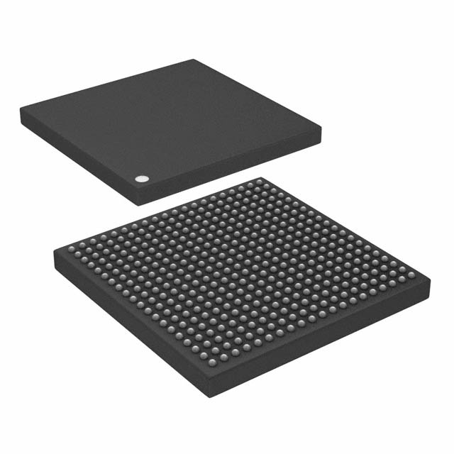
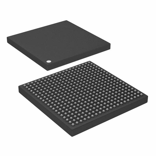
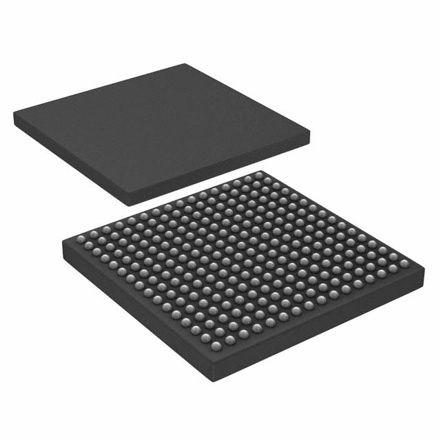
IGLOO2 Field Programmable Gate Array (FPGA) IC 207 1130496 27696 400-LFBGA |
|---|---|
| Quantity | 157 Available (as of October 8, 2026) |

| Product Category | Field Programmable Gate Array (FPGA) |
|---|---|
| Manufacturer | Microchip Technology |
| Manufacturing Status | Active |
| Manufacturer Standard Lead Time | 10 Weeks |
| Datasheet |
Specifications & Environmental
| Device Package | 400-VFBGA (17x17) | Grade | Commercial | Operating Temperature | 0°C – 85°C | ||
|---|---|---|---|---|---|---|---|
| Package / Case | 400-LFBGA | Number of I/O | 207 | Voltage | 1.14 V - 2.625 V | ||
| Mounting Method | Surface Mount | RoHS Compliance | ROHS3 Compliant | REACH Compliance | REACH Unaffected | ||
| Moisture Sensitivity Level | 3 (168 Hours) | Number of LABs/CLBs | 27696 | Number of Logic Elements/Cells | 27696 | ||
| Number of Gates | N/A | ECCN | 3A991D | HTS Code | 8542.39.0001 | ||
| Qualification | N/A | Total RAM Bits | 1130496 |
Overview of M2GL025T-1VFG400 – IGLOO2 Field Programmable Gate Array (FPGA) IC 207 1130496 27696 400-LFBGA
The M2GL025T-1VFG400 is a flash-based IGLOO2 FPGA from Microchip Technology offering a balance of logic capacity, on-chip memory and high-speed interfaces in a compact 400-LFBGA package. Built on the IGLOO2 architecture, this device targets commercial embedded and communications designs that require programmable logic, integrated memory resources and communication interfaces with an emphasis on low power and security.
This part provides 27,696 logic elements and approximately 1.13 Mbits of embedded RAM, together with up to 207 user I/Os and a documented operating voltage range and temperature rating suited to commercial systems.
Key Features
- Core Architecture: Fourth-generation flash-based IGLOO2 FPGA fabric with 4-input LUTs and carry chains for efficient logic implementation and improved performance.
- Logic Capacity: 27,696 logic elements to implement mid-range FPGA designs and custom processing pipelines.
- Embedded Memory: Approximately 1.13 Mbits of on-chip RAM, plus family-level options for large dual-port SRAM blocks and micro SRAM blocks documented in the IGLOO2 series.
- DSP & Mathblocks: Family architecture includes fast mathblock support for signed/unsigned multiplications and accumulation (refer to IGLOO2 family documentation for block counts and detailed capabilities).
- High-Speed Interfaces: IGLOO2 family supports high-speed serial SERDES lanes and protocols such as PCIe and XAUI/XGMII; this family-level functionality enables implementation of high-throughput links when required by system designs.
- Memory Controllers: Family supports HPMS DDR memory controllers (LPDDR/DDR2/DDR3) and soft SDRAM controllers for designs requiring external DRAM interfaces.
- I/O and Voltage Support: 207 user I/Os with multi-standard I/O support documented for the IGLOO2 family; device supply range is specified as 1.14 V to 2.625 V and core is operated at ~1.2 V as indicated in family documentation.
- Package & Mounting: 400-LFBGA package (supplier package 400-VFBGA, 17×17) designed for surface-mount assembly.
- Operating Range & Compliance: Commercial grade with an operating temperature range of 0 °C to 85 °C and RoHS compliance.
- Security & Reliability: IGLOO2 family-level security features include encrypted bitstream support, device certificate and anti-tamper/zeroization capabilities; consult family datasheet for available cryptographic services on premium devices.
Typical Applications
- High-Speed Communications: Implement protocol bridging, SERDES-based links or PCIe endpoints using the IGLOO2 family’s high-speed serial and protocol support.
- Embedded Processing & DSP: Use the device’s logic elements, mathblocks and on-chip RAM for signal processing pipelines, custom accelerators or control logic in commercial embedded products.
- Memory-Intensive Interfaces: Leverage on-chip RAM and family DDR controller support to build controllers and buffering solutions for systems requiring external DRAM access.
- Secure Embedded Systems: Employ the IGLOO2 family security features for designs that require encrypted bitstreams, device authentication and anti-tamper capabilities.
Unique Advantages
- Flash-Based Nonvolatile Fabric: Retains configuration without external configuration memory, simplifying board-level BOM and system boot requirements.
- Significant On-Chip Resources: 27,696 logic elements and approximately 1.13 Mbits of embedded RAM provide room for substantial logic, buffering and state storage on-chip.
- Integrated High-Speed Capabilities: Family-level SERDES, PCIe and DDR controller options enable integration of high-throughput interfaces without extensive external logic.
- Security-Ready Platform: Family security features such as encrypted bitstreams and device certificates support supply-chain assurance and protected intellectual property models.
- Compact Production Package: 400-LFBGA (17×17) surface-mount package supports dense board designs while offering 207 I/Os for flexible system connectivity.
- RoHS Compliant: Meets RoHS requirements for environmental compliance in commercial electronic products.
Why Choose M2GL025T-1VFG400?
The M2GL025T-1VFG400 delivers a balanced combination of programmable logic, embedded memory and family-level high-speed interface capabilities in a commercial-grade IGLOO2 FPGA. It's suited to designers who need mid-range logic capacity alongside on-chip RAM and the option to implement high-speed serial links or external memory controllers.
For commercial embedded and communications systems that benefit from flash-based nonvolatile configuration, security features and a compact 400-LFBGA package, this device offers a scalable platform with documented family-level resources and on-chip integration that reduce external component count and simplify system design.
Request a quote or submit an inquiry for pricing and availability for M2GL025T-1VFG400.
























Date Founded: 1989
Headquarters: Chandler, Arizona, USA
Employees: 22,000+
Revenue: $8.349 Billion
Certifications and Memberships: ISO9001:2015, IATF16949:2016, AS 9100D




