
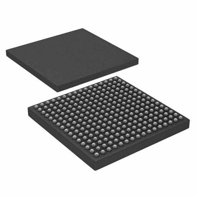
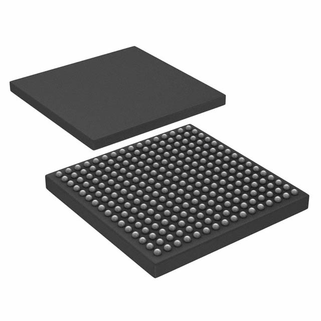
M2GL025TS-1VFG400T2
| Part Description |
IGLOO2 Field Programmable Gate Array (FPGA) IC 207 1130496 27696 |
|---|---|
| Quantity | 1,344 Available (as of October 8, 2026) |

| Product Category | Field Programmable Gate Array (FPGA) |
|---|---|
| Manufacturer | Microchip Technology |
| Manufacturing Status | Active |
| Manufacturer Standard Lead Time | 16 Weeks |
| Datasheet |
Specifications & Environmental
| Device Package | 400-VFBGA (17x17) | Grade | Automotive | Operating Temperature | -40°C – 125°C | ||
|---|---|---|---|---|---|---|---|
| Package / Case | 400-LFBGA | Number of I/O | 207 | Voltage | 1.14 V - 2.625 V | ||
| Mounting Method | Surface Mount | RoHS Compliance | ROHS3 Compliant | REACH Compliance | REACH Unaffected | ||
| Moisture Sensitivity Level | 3 (168 Hours) | Number of LABs/CLBs | 27696 | Number of Logic Elements/Cells | 27696 | ||
| Number of Gates | N/A | ECCN | 5A002A1 | HTS Code | 8542.39.0001 | ||
| Qualification | AEC-Q100 | Total RAM Bits | 1130496 |
Overview of M2GL025TS-1VFG400T2 – IGLOO2 FPGA — 27,696 logic elements, ~1.13 Mbit RAM, 207 I/Os
The M2GL025TS-1VFG400T2 is an IGLOO2 flash-based Field Programmable Gate Array (FPGA) from Microchip Technology. It combines a high-density programmable fabric with embedded memory and high-performance communications and memory interface capabilities targeted at designs that require low power, on-chip memory and robust I/O.
This device is suitable for designs that demand substantial logic resources (27,696 logic elements), significant on-chip RAM (approximately 1.13 Mbits), and a broad I/O complement (207 I/Os). Packaging, voltage range and qualification details support deployment in temperature- and reliability-sensitive applications.
Key Features
- Programmable Fabric Efficient 4-input LUT architecture with carry chains and a reported 27,696 logic elements for implementing complex logic functions.
- On-Chip Memory Approximately 1.13 Mbits of total RAM bits on-chip, with IGLOO2 family memory options including embedded SRAM and nonvolatile memory blocks for application buffering and storage.
- DSP and Math Resources IGLOO2 family architecture provides dedicated mathblocks for signed/unsigned multiplication and accumulation to accelerate digital signal processing tasks.
- High-Speed Serial and Parallel Interfaces 207 user I/Os and family support for high-speed serial SERDES lanes, PCI Express, XAUI/XGXS and multi-standard user I/O signaling to address a wide range of interface requirements.
- High-Speed Memory Controllers IGLOO2 family supports DDRx memory controllers (LPDDR/DDR2/DDR3) and flexible DRAM bus-width modes for high-bandwidth external memory access.
- Security and Reliability Features Family-level design and data security features include encrypted bitstream loading, device certificate support and cryptographic services on premium devices (e.g., AES-256, SHA-256, ECC and NRBG options).
- Power and Voltage Supports a device voltage range from 1.14 V to 2.625 V, enabling flexible power-domain integration in multi-voltage systems.
- Package and Mounting Supplied in a 400-LFBGA (400-VFBGA 17×17) package for surface-mount assembly.
- Automotive Qualification and Temperature Range Automotive grade device qualified to AEC-Q100 with an operating temperature range of −40 °C to 125 °C.
- Compliance RoHS compliant.
Typical Applications
- Automotive Systems Leverage automotive qualification and extended temperature operation for vehicle subsystems such as infotainment interface logic, gateway or sensor aggregation where on-chip logic and security matter.
- High-Speed Communications Implement 10 Gbps-class PHY interfaces, PCIe endpoints or multi-lane SERDES links using the IGLOO2 family’s high-speed serial and protocol capabilities.
- Memory-Intensive Embedded Designs Use on-chip RAM combined with DDRx controllers to support buffering, frame storage or fast data staging in embedded controllers and data acquisition systems.
- Signal Processing and DSP Offload Accelerate math-heavy functions and real-time processing using the family’s dedicated mathblocks and embedded memory resources.
Unique Advantages
- High Logic Density: 27,696 logic elements provide substantial programmable capacity for complex control, interface and processing tasks.
- Significant On-Chip Memory: Approximately 1.13 Mbits of embedded RAM reduces reliance on external memory for many buffering and scratch requirements.
- Automotive-Grade Qualification: AEC-Q100 qualification and −40 °C to 125 °C operating range enable use in temperature- and reliability-sensitive automotive applications.
- Flexible I/O and Voltage Support: 207 user I/Os and supply range from 1.14 V to 2.625 V allow integration with a variety of interfaces and system power domains.
- Integrated High-Speed Interfaces: Family-level support for SERDES, PCIe and DDRx controllers simplifies implementation of high-bandwidth communication and memory subsystems.
- Security Capabilities: Built-in design and data security options help protect IP and support secure boot/bitstream workflows on applicable devices.
Why Choose M2GL025TS-1VFG400T2?
The M2GL025TS-1VFG400T2 packs a large programmable fabric, meaningful on-chip memory and a broad I/O set into a 400-LFBGA package with automotive qualification. It is positioned for engineers who need a secure, memory-capable FPGA with extensive interface options and the environmental robustness required for automotive and other temperature-sensitive deployments.
For designs that require integration of high-speed interfaces, DSP acceleration and on-chip buffering while maintaining automotive-grade qualification, this IGLOO2 device offers a balanced combination of logic capacity, memory and system-level features aligned to those requirements.
Request a quote or submit an inquiry to get pricing, lead times and availability for the M2GL025TS-1VFG400T2.





















Date Founded: 1989
Headquarters: Chandler, Arizona, USA
Employees: 22,000+
Revenue: $8.349 Billion
Certifications and Memberships: ISO9001:2015, IATF16949:2016, AS 9100D




