
XC4005XL-3PC84C
| Part Description |
XC4000E/X Field Programmable Gate Array (FPGA) IC 61 6272 466 84-LCC (J-Lead) |
|---|---|
| Quantity | 347 Available (as of October 8, 2026) |

| Product Category | Field Programmable Gate Array (FPGA) |
|---|---|
| Manufacturer | AMD |
| Manufacturing Status | Obsolete |
| Manufacturer Standard Lead Time | Contact Us |
| Datasheet |
Specifications & Environmental
| Device Package | 84-PLCC (29.31x29.31) | Grade | Commercial | Operating Temperature | 0°C – 85°C | ||
|---|---|---|---|---|---|---|---|
| Package / Case | 84-LCC (J-Lead) | Number of I/O | 61 | Voltage | 3 V - 3.6 V | ||
| Mounting Method | Surface Mount | RoHS Compliance | RoHS non-compliant | REACH Compliance | REACH Unaffected | ||
| Moisture Sensitivity Level | 3 (168 Hours) | Number of LABs/CLBs | 196 | Number of Logic Elements/Cells | 466 | ||
| Number of Gates | 5000 | ECCN | EAR99 | HTS Code | 8542.39.0001 | ||
| Qualification | N/A | Total RAM Bits | 6272 |
Overview of XC4005XL-3PC84C – XC4000E/X Field Programmable Gate Array (FPGA), 61 I/O, 466 Logic Elements, 84-LCC
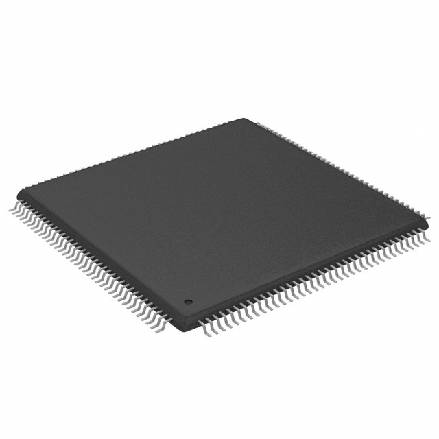
The XC4005XL-3PC84C is a Field Programmable Gate Array (FPGA) IC from AMD’s XC4000E/X family provided in an 84-lead LCC (J-lead) surface-mount package. It delivers a compact, reprogrammable logic solution with 466 logic elements, 6,272 bits of embedded RAM and 61 user I/O pins for mid-density programmable logic tasks.
Designed for commercial-grade applications, the device operates from a 3.0 V to 3.6 V supply and across a 0 °C to 85 °C temperature range. It is RoHS compliant and suited to designs where moderate gate count, on-chip RAM and flexible I/O are primary requirements.
Key Features
- Core Architecture FPGA device from the XC4000E/X family provided in the XC4005XL variant—engineered for reprogrammable, mid-density logic implementations.
- Logic Capacity 466 logic elements that enable implementation of a range of combinational and sequential logic functions.
- Embedded Memory 6,272 bits of on-chip RAM to support small data buffering, state storage and lookup-table requirements.
- I/O 61 user I/O pins for interfacing with peripherals, sensors and other digital subsystems.
- Gate Count Approximately 5,000 gates of equivalent logic capacity for mid-range design complexity.
- Power Single-supply operation from 3.0 V to 3.6 V for compatibility with common digital power rails.
- Package & Mounting 84-lead LCC (J-lead) surface-mount package; supplier device package listed as 84-PLCC (29.31 × 29.31 mm).
- Temperature & Grade Commercial grade operation from 0 °C to 85 °C for standard environmental conditions.
- Environmental Compliance RoHS compliant for alignment with lead-free product requirements.
Typical Applications
- Logic Prototyping and Development Reprogrammable logic elements and on-chip RAM make the device suitable for validating digital designs and prototypes.
- Control and Sequencing Use the FPGA to implement finite state machines, control logic and timing sequencers that require flexible reconfiguration.
- Interface Bridging 61 I/O pins provide the connectivity needed to implement protocol translation and glue logic between subsystems.
- Embedded Feature Offload Offload mid-complexity functions from a microcontroller to dedicated programmable logic to free CPU resources.
Unique Advantages
- Compact, mid-density FPGA: 466 logic elements and ~5,000 gates provide a balanced option for designs that need more capability than simple CPLDs but do not require high-density FPGAs.
- On-chip RAM available: 6,272 bits of embedded memory simplify small buffering and state storage without external RAM, reducing BOM and board area.
- Generous I/O count: 61 user I/O pins support multiple peripheral connections and flexible board partitioning.
- Standard commercial operating range: 0 °C to 85 °C operation aligns with mainstream electronics and consumer applications.
- Lead-free compliant: RoHS compliance supports contemporary environmental requirements and manufacturing processes.
- Surface-mount 84-LCC package: Provides a compact footprint for PCB assembly while offering the robustness of a J-lead package.
Why Choose XC4005XL-3PC84C?
The XC4005XL-3PC84C positions itself as a practical, reprogrammable solution for mid-density digital designs where a combination of logic elements, embedded RAM and a moderate I/O count are required. Its 3.0–3.6 V supply range and commercial temperature rating make it straightforward to integrate into standard digital systems.
This FPGA is well suited to engineering teams and procurement looking for a compact, RoHS-compliant device that balances integration and flexibility without moving into higher-density, higher-cost families. Use it in projects requiring reprogrammable logic, modest on-chip memory and flexible interfacing in a surface-mount 84-lead LCC package.
If you would like pricing or availability information for the XC4005XL-3PC84C, request a quote or submit an inquiry and our team will respond with details and ordering options.























Date Founded: 1969
Headquarters: Santa Clara, California, USA
Employees: 25,000+
Revenue: $22.68 Billion
Certifications and Memberships: ISO9001:2015, RoHS, REACH











