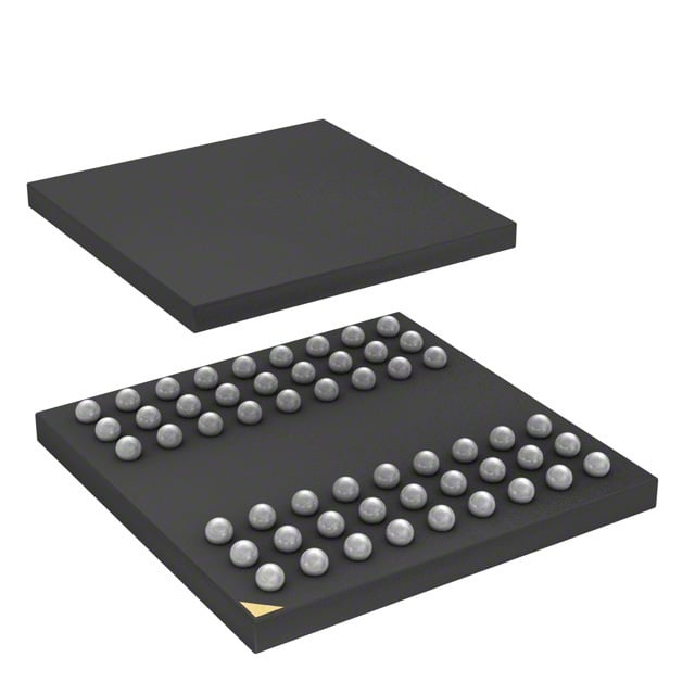
AS4C16M16SA-7BCN
| Part Description |
IC DRAM 256MBIT PAR 54TFBGA |
|---|---|
| Quantity | 470 Available (as of June 15, 2026) |

| Product Category | Memory |
|---|---|
| Manufacturer | Alliance Memory, Inc. |
| Manufacturing Status | Active |
| Manufacturer Standard Lead Time | 6 Weeks |
| Datasheet |
Specifications & Environmental
| Device Package | 54-TFBGA (8x8) | Memory Format | DRAM | Technology | SDRAM | ||
|---|---|---|---|---|---|---|---|
| Memory Size | 256 Mbit | Access Time | 5.4 ns | Grade | Commercial | ||
| Clock Frequency | 143 MHz | Voltage | 3V ~ 3.6V | Memory Type | Volatile | ||
| Operating Temperature | 0°C ~ 70°C (TA) | Write Cycle Time Word Page | 14 ns | Packaging | 54-TFBGA | ||
| Mounting Method | Volatile | Memory Interface | Parallel | Memory Organization | 16M x 16 | ||
| Moisture Sensitivity Level | 3 (168 Hours) | RoHS Compliance | ROHS Compliant | REACH Compliance | REACH Unaffected | ||
| Qualification | N/A | ECCN | EAR99 | HTS Code | 8542.32.0024 |
Overview of AS4C16M16SA-7BCN – IC DRAM 256MBIT PAR 54TFBGA
The AS4C16M16SA-7BCN is a 256 Mbit volatile DRAM device implemented in SDRAM architecture with a parallel memory interface. It is organized as 16M × 16 bits and supplied in a 54‑TFBGA (8×8) package.
This device targets designs that require a moderate-density parallel SDRAM solution with defined electrical and timing characteristics: a clock frequency up to 143 MHz, 5.4 ns access time, and a write cycle time of 14 ns, operating from 3.0 V to 3.6 V and across an ambient temperature range of 0 °C to 70 °C.
Key Features
- Memory Type & Technology Volatile SDRAM architecture providing standard DRAM behavior for temporary data storage.
- Organization & Density 16M × 16 organization yielding a total memory size of 256 Mbit.
- Interface Parallel memory interface suitable for parallel DRAM subsystem designs.
- Performance Clock frequency up to 143 MHz with a listed access time of 5.4 ns and a write cycle time (word page) of 14 ns.
- Power Operating voltage range from 3.0 V to 3.6 V.
- Package 54‑TFBGA package (8×8) providing a compact ball grid array footprint.
- Operating Conditions Specified ambient operating temperature range of 0 °C to 70 °C.
Typical Applications
- Parallel memory subsystems Use as a 256 Mbit parallel SDRAM device in boards and modules that require 16M × 16 memory organization.
- External DRAM for processors Provides temporary data storage for processors and controllers that interface with parallel SDRAM.
- Compact board-level designs The 54‑TFBGA (8×8) package supports space-constrained PCB layouts needing moderate-density volatile memory.
Unique Advantages
- 256 Mbit density in a compact package: 16M × 16 organization in a 54‑TFBGA (8×8) package balances capacity with board space efficiency.
- Deterministic timing data: Specified 5.4 ns access time and 14 ns write cycle time enable predictable performance analysis.
- Defined clock capability: Rated for operation up to 143 MHz to support designs targeting that operating frequency.
- Standard SDRAM technology: Uses SDRAM architecture for conventional volatile memory behavior and system integration.
- Wide supply tolerance: 3.0 V to 3.6 V supply range accommodates standard 3 V power domains.
- Specified operating range: 0 °C to 70 °C ambient rating for applications within this temperature envelope.
Why Choose AS4C16M16SA-7BCN?
The AS4C16M16SA-7BCN provides a straightforward, specification-driven SDRAM option for designs requiring 256 Mbit of parallel volatile memory in a 16M × 16 organization. Its documented timing (5.4 ns access, 14 ns write cycle) and clock rating (143 MHz) allow engineers to plan memory subsystem performance precisely.
This device is suited for board- and module-level implementations that need a compact 54‑TFBGA package and standard 3.0–3.6 V operation across a 0 °C to 70 °C ambient range, offering a clear set of electrical and mechanical parameters for integration and qualification.
Request a quote or contact sales to discuss pricing, availability, and lead times for AS4C16M16SA-7BCN.