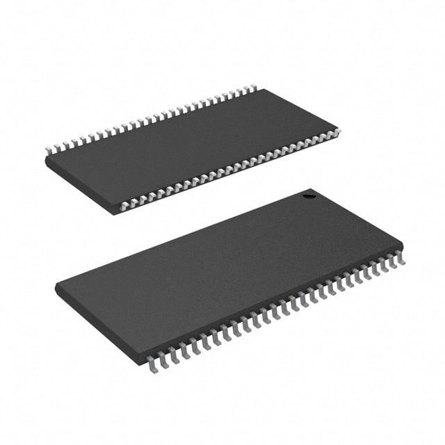
AS4C16M16SA-6TCN
| Part Description |
IC DRAM 256MBIT PAR 54TSOP II |
|---|---|
| Quantity | 870 Available (as of June 15, 2026) |

| Product Category | DRAM Memory |
|---|---|
| Manufacturer | Alliance Memory, Inc. |
| Manufacturing Status | Active |
| Manufacturer Standard Lead Time | 8 Weeks |
| Datasheet |
Specifications & Environmental
| Device Package | 54-TSOP II | Memory Format | DRAM | Technology | SDRAM | ||
|---|---|---|---|---|---|---|---|
| Memory Size | 256 Mbit | Access Time | 5 ns | Grade | Commercial | ||
| Clock Frequency | 166 MHz | Voltage | 3V ~ 3.6V | Memory Type | Volatile | ||
| Operating Temperature | 0°C ~ 70°C (TA) | Write Cycle Time Word Page | 12 ns | Packaging | 54-TSOP (0.400", 10.16mm Width) | ||
| Mounting Method | Volatile | Memory Interface | Parallel | Memory Organization | 16M x 16 | ||
| Moisture Sensitivity Level | 3 (168 Hours) | RoHS Compliance | ROHS Compliant | REACH Compliance | REACH Unaffected | ||
| Qualification | N/A | ECCN | EAR99 | HTS Code | 8542.32.0024 |
Overview of AS4C16M16SA-6TCN - 256Mbit Parallel SDRAM
The AS4C16M16SA-6TCN is a 256-megabit synchronous DRAM organized as 16M x 16, delivering reliable memory performance for embedded systems and computing applications. Built on proven SDRAM technology, this device operates at up to 166MHz clock frequency with a 5ns access time, making it well-suited for applications requiring predictable memory timing and moderate bandwidth.
With its 3V to 3.6V supply voltage and commercial temperature range, the AS4C16M16SA-6TCN provides a cost-effective memory solution for industrial controls, communications equipment, and general-purpose computing platforms where standard operating conditions apply.
Key Features
- Memory Architecture - 256Mbit capacity organized as 16 million words by 16 bits, providing flexible word-level access for 16-bit and 32-bit processor architectures.
- Performance Specifications - 166MHz maximum clock frequency with 5ns access time and 12ns write cycle time, delivering consistent timing for synchronous system designs.
- Power Supply - Standard 3V to 3.6V operation simplifies integration with common logic families and reduces power distribution complexity.
- Parallel Interface - Traditional parallel memory interface with synchronous clocking for straightforward integration with existing memory controller designs.
- Package Configuration - 54-pin TSOP II package (10.16mm width) offers industry-standard footprint compatible with widely-used PCB layouts.
- Operating Environment - Commercial temperature range of 0°C to 70°C supports deployment in climate-controlled equipment and standard operating environments.
Typical Applications
- Embedded Computing Systems - This SDRAM serves as main memory or buffer storage in embedded processors and microcontrollers, where its synchronous operation aligns with system clock domains for deterministic timing behavior.
- Industrial Control Equipment - Provides data buffering and program storage for PLCs and industrial controllers operating in temperature-controlled environments, where the parallel interface simplifies legacy system integration.
- Communications Infrastructure - Functions as packet buffering and routing table memory in networking equipment, where the 166MHz operation supports moderate throughput requirements in managed switches and routers.
- Test and Measurement Instruments - Offers waveform storage and data acquisition buffering in benchtop instruments, where the predictable access timing facilitates precise sample capture and analysis.
- Consumer Electronics - Supports set-top boxes, digital displays, and multimedia devices operating in indoor environments, where cost-effective memory density meets typical system requirements.
Unique Advantages
- Industry-Standard Architecture: Proven SDRAM technology with widely supported parallel interface reduces design risk and leverages existing controller IP and driver software.
- Simplified Supply Design: Single 3V to 3.6V power rail eliminates need for multiple voltage regulators, reducing BOM cost and board complexity.
- Established Footprint Compatibility: Standard 54-TSOP II package enables drop-in replacement opportunities and reuse of proven PCB layouts from previous designs.
- Predictable Performance Characteristics: Synchronous clocking with specified access and cycle times facilitates straightforward timing analysis and controller configuration.
- Cost-Effective Density: 256Mbit capacity in a single component reduces component count compared to multiple smaller devices while meeting moderate memory requirements.
- Active Lifecycle Status: Ongoing production availability supports long-term procurement for products with multi-year lifecycles and replacement part requirements.
Why Choose AS4C16M16SA-6TCN?
The AS4C16M16SA-6TCN represents a practical choice for designs requiring proven memory technology with straightforward integration. Its parallel SDRAM architecture offers compatibility with established controller designs and extensive driver support, reducing development time and technical risk. The standard supply voltage and package footprint facilitate design reuse and component sourcing flexibility.
This device is particularly well-suited for embedded systems, industrial equipment, and commercial electronics operating in controlled environments where reliable synchronous memory is needed at competitive cost. Engineers working on upgrades to existing platforms or new designs with moderate memory requirements will find the AS4C16M16SA-6TCN delivers the functionality and availability needed for successful product deployment.
Get a Quote Today
Contact our technical sales team to discuss your memory requirements and receive pricing for the AS4C16M16SA-6TCN. Our specialists can provide application guidance, availability information, and volume pricing to support your project timeline and budget.