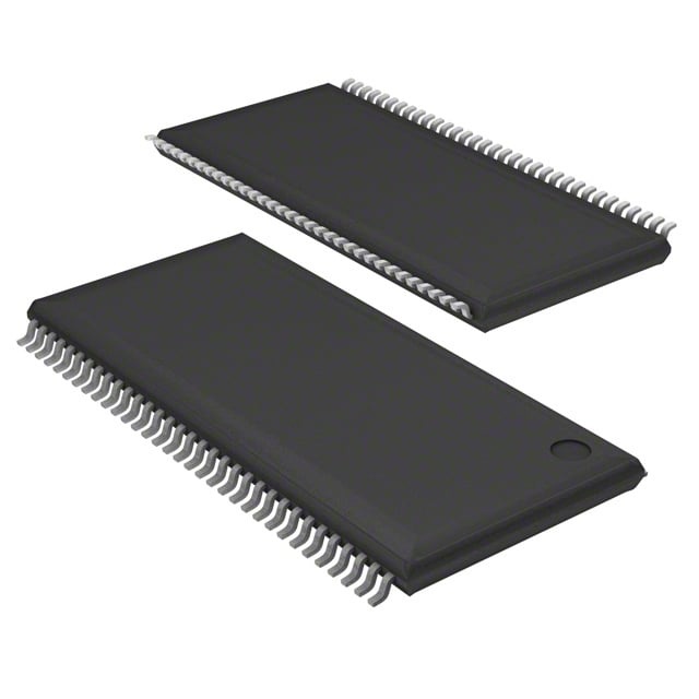
AS4C32M16D1-5TIN
| Part Description |
IC DRAM 512MBIT PAR 66TSOP II |
|---|---|
| Quantity | 818 Available (as of June 15, 2026) |

| Product Category | DRAM Memory |
|---|---|
| Manufacturer | Alliance Memory, Inc. |
| Manufacturing Status | Obsolete |
| Manufacturer Standard Lead Time | Contact Us |
| Datasheet |
Specifications & Environmental
| Device Package | 66-TSOP II | Memory Format | DRAM | Technology | SDRAM - DDR | ||
|---|---|---|---|---|---|---|---|
| Memory Size | 512 Mbit | Access Time | 700 ps | Grade | Industrial | ||
| Clock Frequency | 200 MHz | Voltage | 2.3V ~ 2.7V | Memory Type | Volatile | ||
| Operating Temperature | -40°C ~ 85°C (TA) | Write Cycle Time Word Page | 15 ns | Packaging | 66-TSSOP (0.400", 10.16mm Width) | ||
| Mounting Method | Volatile | Memory Interface | Parallel | Memory Organization | 32M x 16 | ||
| Moisture Sensitivity Level | 3 (168 Hours) | RoHS Compliance | ROHS3 Compliant | REACH Compliance | REACH Unaffected | ||
| Qualification | N/A | ECCN | 3A991B2A | HTS Code | 8542.32.0028 |
Overview of AS4C32M16D1-5TIN – 512Mbit DDR Synchronous DRAM, 66‑Pin TSOP II
The AS4C32M16D1-5TIN is a 512 Mbit DDR synchronous DRAM organized as 32M × 16 bits. It implements a DDR architecture with differential clocks and bidirectional DQS to deliver synchronous, burst-oriented memory access for systems that require high memory bandwidth.
This industrial-temperature device (‑40 °C to 85 °C) is supplied in a 66‑pin TSOP II (0.65 mm pitch) package and targets applications and designs needing parallel DDR memory with configurable latency and burst modes.
Key Features
- Memory Organization & Capacity — 512 Mbit total capacity, internally configured as four banks of 8M × 16 bits (32M × 16 organization).
- DDR Synchronous Architecture — Double data rate operation with differential CK/CK̄ and bi‑directional DQS for data capture on both clock edges.
- Performance — 200 MHz clock frequency (400 Mbps per pin data rate) with an access time of 700 ps and a write cycle time (word/page) of 15 ns.
- Programmable Modes — Mode and Extended Mode registers support programmable CAS latencies (2, 2.5, 3), burst lengths (2, 4, 8) and burst type (sequential or interleaved).
- Data Integrity & Control — Individual byte‑write mask control, DM write latency = 0, and support for Auto Refresh and Self Refresh (8192 refresh cycles per 64 ms).
- Power & Interface — VDD and VDDQ nominal 2.5 V (specified 2.3 V – 2.7 V range). SSTL_2 I/O interface compatibility is specified in the device documentation.
- Package & Temperature — 66‑pin TSOP II (0.400" / 10.16 mm width, 0.65 mm pin pitch), rated for industrial ambient operation from ‑40 °C to 85 °C.
- Configuration Options — DLL enable/disable via Extended Mode Register and support for programmable features to optimize timing for target systems.
Typical Applications
- Industrial Control Systems — Use the industrial temperature range and DDR throughput for memory buffers and high‑speed data buffering in industrial modules.
- High‑Bandwidth Embedded Modules — Suitable for embedded designs requiring synchronous burst access and configurable latency/burst modes to match system timing.
- Memory Subsystems — Acts as a parallel DDR memory component in multi‑bank memory architectures that need predictable refresh and burst behavior.
Unique Advantages
- High throughput: 200 MHz clock supporting 400 Mbps per pin enables sustained burst transfers for bandwidth‑sensitive tasks.
- Flexible timing configuration: Multiple CAS latencies and burst lengths allow tuning for performance vs. system timing constraints.
- Robust refresh management: Auto and Self Refresh with 8192 cycles/64 ms simplifies maintenance of data integrity across operating conditions.
- Industrial temperature rating: Specified operation from ‑40 °C to 85 °C supports deployment in temperature‑challenging environments.
- Compact package: 66‑pin TSOP II offers a space‑efficient footprint for board designs requiring parallel DDR memory.
- Low‑voltage DDR operation: 2.3 V – 2.7 V supply range aligns with common low‑voltage memory system rails.
Why Choose IC DRAM 512MBIT PAR 66TSOP II?
The AS4C32M16D1-5TIN provides a configurable DDR SDRAM solution combining 512 Mbit capacity, multi‑bank organization, and programmable timing to meet a range of embedded and industrial memory requirements. Its DDR interface (differential clock and DQS), selectable CAS latencies, and burst controls let system designers balance bandwidth and timing for targeted applications.
This device is suited to designs that need parallel DDR memory in a compact 66‑pin TSOP II package with industrial temperature support and standard low‑voltage supply ranges, offering predictable refresh behavior and configurable operation for long‑term system stability.
Request a quote or contact sales to discuss availability, volume pricing, and lead‑time options for the AS4C32M16D1-5TIN.