AS4C32M16D2-25BIN
| Part Description |
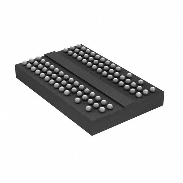
IC DRAM 512MBIT PAR 84TFBGA |
|---|---|
| Quantity | 770 Available (as of June 15, 2026) |

| Product Category | Memory |
|---|---|
| Manufacturer | Alliance Memory, Inc. |
| Manufacturing Status | Obsolete |
| Manufacturer Standard Lead Time | Contact Us |
| Datasheet |
Specifications & Environmental
| Device Package | 84-TFBGA (8x12.5) | Memory Format | DRAM | Technology | SDRAM - DDR2 | ||
|---|---|---|---|---|---|---|---|
| Memory Size | 512 Mbit | Access Time | 400 ps | Grade | Automotive | ||
| Clock Frequency | 400 MHz | Voltage | 1.7V ~ 1.9V | Memory Type | Volatile | ||
| Operating Temperature | -40°C ~ 95°C (TC) | Write Cycle Time Word Page | 15 ns | Packaging | 84-TFBGA | ||
| Mounting Method | Volatile | Memory Interface | Parallel | Memory Organization | 32M x 16 | ||
| Moisture Sensitivity Level | 3 (168 Hours) | RoHS Compliance | ROHS3 Compliant | REACH Compliance | REACH Unaffected | ||
| Qualification | N/A | ECCN | 3A991B2A | HTS Code | 8542.32.0028 |
Overview of AS4C32M16D2-25BIN – IC DRAM 512MBIT PAR 84TFBGA
The AS4C32M16D2-25BIN is a 512 Mbit DDR2 synchronous DRAM organized as 32M x 16 bits. It implements a quad-bank, 4-bit prefetch architecture with a fully synchronous, pipelined DDR2 interface targeted at systems requiring high-rate parallel memory.
This industrial-temperature device supports a 400 MHz clock (800 Mbps/pin), differential CK/CK# clocks, bidirectional DQS/DQS# strobes and on-die termination, making it suitable for designs that require a compact 84-ball TFBGA memory component with extended temperature operation.
Key Features
- Core / Architecture Quad-bank DDR2 SDRAM with internal pipeline architecture and 4-bit prefetch; organized as 32M × 16 I/Os for a total of 512 Mbit.
- Memory Performance JEDEC-compliant DDR2 operation with a fast clock rate of 400 MHz (800 Mbps per pin), burst lengths 4 or 8, and programmable CAS/additive latencies.
- Interface & Timing Differential clock inputs (CK/CK#), bidirectional data strobes (DQS/DQS#), posted CAS# additive latency, and WRITE latency = READ latency − 1 tCK; typical write cycle time (word page) 15 ns.
- Power JEDEC standard 1.8 V I/O with VDD and VDDQ = +1.8 V ±0.1 V (specified supply range 1.7 V to 1.9 V).
- Signal Conditioning On-die termination (ODT), Off-Chip Driver (OCD) impedance adjustment and adjustable data-output drive strength to aid signal integrity.
- Reliability & Refresh Auto-refresh and self-refresh supported with 8192 refresh cycles/64 ms and temperature-dependent average refresh periods as specified in the device documentation.
- Package 84-ball thin FBGA (8.0 × 12.5 × 1.2 mm max) package (84-TFBGA) for compact mounting.
- Temperature Range & Compliance Industrial operating temperature −40 °C to +95 °C; device listing indicates RoHS compliance and Pb and halogen free construction.
Typical Applications
- Industrial Equipment Use in systems that require memory components rated for −40 °C to +95 °C operating environments.
- Embedded Memory Subsystems Parallel DDR2 memory for embedded boards and modules that need a 512 Mbit, 16-bit wide DRAM interface.
- High-Speed Data Buffers Applications requiring 800 Mbps/pin data transfers with differential clocking and source-synchronous DQS signaling.
Unique Advantages
- High data-rate DDR2 interface: 400 MHz clock (800 Mbps/pin) supports high-throughput parallel data transfer.
- Industrial temperature rating: Specified −40 °C to +95 °C for deployment in extended-temperature systems.
- Integrated signal integrity controls: On-die termination, OCD impedance adjustment, and adjustable output drive strength reduce board-level tuning effort.
- Compact FBGA package: 84-ball 8.0 × 12.5 × 1.2 mm TFBGA provides a small footprint for space-constrained designs.
- JEDEC standard compliance: Standard DDR2 features and timing options (burst lengths, CAS/additive latency) enable predictable integration into DDR2 memory subsystems.
- RoHS and Pb/halogen-free construction: Meets environmental material requirements noted in the device documentation.
Why Choose AS4C32M16D2-25BIN?
The AS4C32M16D2-25BIN delivers a JEDEC-compliant DDR2 memory building block combining 512 Mbit capacity, a 16-bit data path, and 400 MHz clock operation in a compact 84-TFBGA package. Its combination of differential clocking, source-synchronous DQS strobes, on-die termination and adjustable drive strength supports reliable high-speed operation in designs that require deterministic DDR2 behavior.
This industrial-temperature device is suited to engineers specifying parallel DDR2 memory for embedded and industrial systems where small footprint, standard DDR2 timing modes, and extended operating temperature are required. The documented electrical and timing features help simplify board-level integration and system validation over the product lifecycle.
Request a quote or submit a specification inquiry to discuss availability, pricing and design-level questions for the AS4C32M16D2-25BIN.