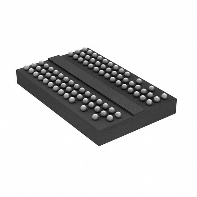
AS4C32M16D2-25BCN
| Part Description |
IC DRAM 512MBIT PAR 84TFBGA |
|---|---|
| Quantity | 1,168 Available (as of June 15, 2026) |

| Product Category | Memory |
|---|---|
| Manufacturer | Alliance Memory, Inc. |
| Manufacturing Status | Obsolete |
| Manufacturer Standard Lead Time | Contact Us |
| Datasheet |
Specifications & Environmental
| Device Package | 84-TFBGA (8x12.5) | Memory Format | DRAM | Technology | SDRAM - DDR2 | ||
|---|---|---|---|---|---|---|---|
| Memory Size | 512 Mbit | Access Time | 400 ps | Grade | Commercial (Extended) | ||
| Clock Frequency | 400 MHz | Voltage | 1.7V ~ 1.9V | Memory Type | Volatile | ||
| Operating Temperature | 0°C ~ 85°C (TC) | Write Cycle Time Word Page | 15 ns | Packaging | 84-TFBGA | ||
| Mounting Method | Volatile | Memory Interface | Parallel | Memory Organization | 32M x 16 | ||
| Moisture Sensitivity Level | 3 (168 Hours) | RoHS Compliance | ROHS3 Compliant | REACH Compliance | REACH Unaffected | ||
| Qualification | N/A | ECCN | 3A991B2A | HTS Code | 8542.32.0028 |
Overview of AS4C32M16D2-25BCN – IC DRAM 512MBIT PAR 84TFBGA
The AS4C32M16D2-25BCN is a 512 Mbit DDR2 synchronous DRAM organized as 32M × 16 bits. It implements a quad-bank architecture with a 4-bit prefetch and internal pipeline to support high-speed DDR2 operation.
Designed for JEDEC-compliant DDR2 memory subsystems, this device targets commercial-temperature applications requiring a 1.8 V I/O interface and a fast clock rate up to 400 MHz (800 Mbps/pin). It is supplied in an 84-ball TFBGA package (8.0 × 12.5 × 1.2 mm).
Key Features
- Memory Core 512 Mbit capacity, organized as 32M × 16 bits with 4 internal banks for concurrent operation.
- DDR2 Architecture Double-Data-Rate-Two (DDR2) synchronous operation with a 4-bit prefetch and internal pipeline architecture.
- Performance Fast clock rate: 400 MHz (800 Mbps/pin); access time listed as 400 ps and write cycle time (word page) of 15 ns.
- Interface & Timing Differential clock inputs (CK & CK#), bidirectional data strobes (DQS & DQS#), burst lengths of 4 or 8, and programmable posted CAS additive latency (AL = 0–6).
- Power & Voltage JEDEC standard 1.8 V I/O (VDD & VDDQ = +1.8 V ± 0.1 V) with support for precharge and active power-down modes, auto refresh and self refresh.
- Signal Integrity & Drive On-Die Termination (ODT), Off-Chip Driver (OCD) impedance adjustment, and adjustable data-output drive strength.
- Reliability & Refresh 8192 refresh cycles/64 ms with specified average refresh periods across the commercial temperature range.
- Package & Temperature 84-ball TFBGA (8.0 × 12.5 × 1.2 mm) in commercial temperature grade: 0°C to +85°C. Pb and halogen free / RoHS compliant.
Typical Applications
- DDR2 memory subsystems Used as a 1.8 V, 512 Mbit DDR2 component in system memory designs targeting 800 Mbps/pin operation.
- Board-level memory integration Suitable for integration onto memory modules or system boards requiring an 84-ball TFBGA DDR2 device.
- Commercial embedded systems Appropriate for commercial-temperature designs (0°C to +85°C) needing synchronous DDR2 storage with programmable latency and burst operation.
Unique Advantages
- High data-rate capability: Supports 400 MHz clocking (800 Mbps/pin) for designs requiring elevated DDR2 throughput.
- Flexible latency and burst control: Programmable posted CAS additive latency (0–6), selectable burst lengths (4 or 8) and burst type (sequential/interleave) to tune system timing.
- On-chip signal conditioning: On-Die Termination, Off-Chip Driver impedance adjustment and adjustable drive strength improve signal integrity options.
- Power-management features: Auto refresh, self refresh, and active/precharge power-down modes help manage power in system implementations.
- Compact package: 84-ball TFBGA (8.0 × 12.5 × 1.2 mm) provides a small footprint for board-level memory integration.
- Standards compliance: JEDEC standard compliant DDR2 interface and JEDEC 1.8 V I/O compatibility for predictable system integration.
Why Choose AS4C32M16D2-25BCN?
The AS4C32M16D2-25BCN delivers a JEDEC-compliant DDR2 solution with 512 Mbit density, 4-bank organization and features such as ODT, OCD impedance adjustment and programmable latencies. Its 400 MHz clock rating and 4-bit prefetch architecture make it suitable for commercial designs that require synchronous DDR2 performance at 1.8 V supply levels.
Packaged in an 84-ball TFBGA and specified for 0°C to +85°C operation, this device is intended for board-level integration where predictable DDR2 timing, configurable drive and termination options, and standard-compliant operation are required.
Request a quote or contact sales to discuss availability, lead times and volume pricing for the AS4C32M16D2-25BCN.