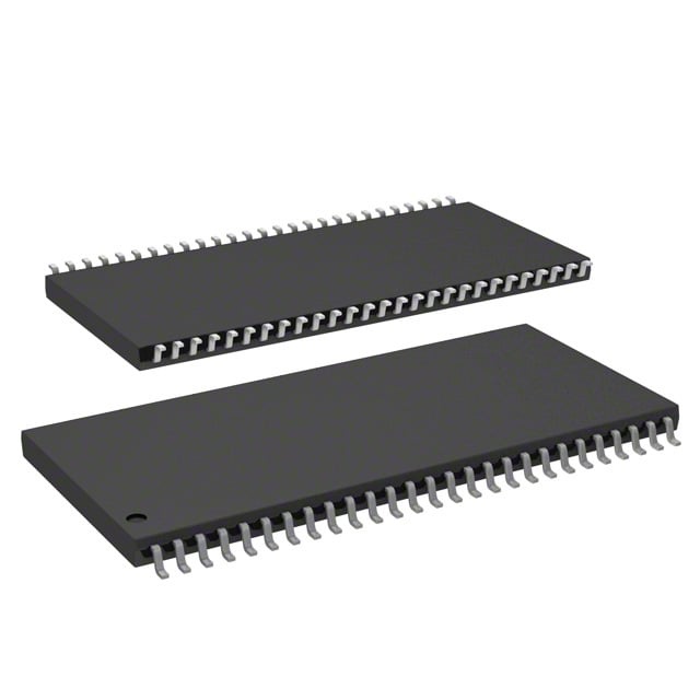
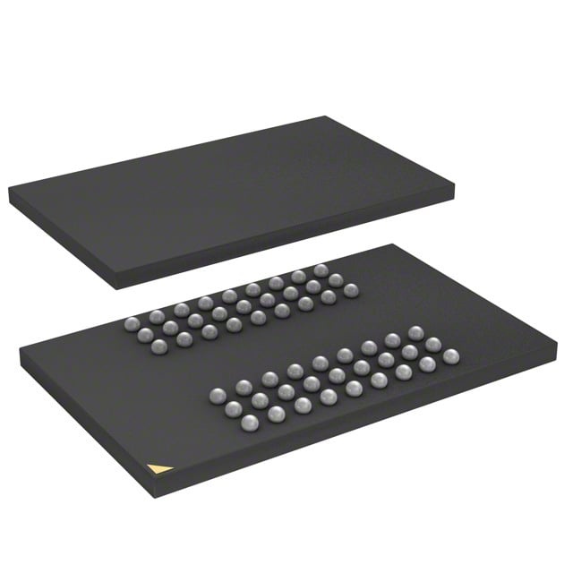
IS42S16160B-7BL
| Part Description |
IC DRAM 256MBIT PAR 54LFBGA |
|---|---|
| Quantity | 1,056 Available (as of June 15, 2026) |
| Product Category | DRAM Memory |
|---|---|
| Manufacturer | Integrated Silicon Solution Inc |
| Manufacturing Status | Obsolete |
| Manufacturer Standard Lead Time | Contact Us |
| Datasheet |
Specifications & Environmental
| Device Package | 54-LFBGA (8x13) | Memory Format | DRAM | Technology | SDRAM | ||
|---|---|---|---|---|---|---|---|
| Memory Size | 256 Mbit | Access Time | 5.4 ns | Grade | Commercial | ||
| Clock Frequency | 143 MHz | Voltage | 3V ~ 3.6V | Memory Type | Volatile | ||
| Operating Temperature | 0°C ~ 70°C (TA) | Write Cycle Time Word Page | N/A | Packaging | 54-LFBGA | ||
| Mounting Method | Volatile | Memory Interface | Parallel | Memory Organization | 16M x 16 | ||
| Moisture Sensitivity Level | 3 (168 Hours) | RoHS Compliance | ROHS3 Compliant | REACH Compliance | REACH Unaffected | ||
| Qualification | N/A | ECCN | EAR99 | HTS Code | 8542.32.0024 |
Overview of IS42S16160B-7BL – IC DRAM 256MBIT PAR 54LFBGA
The IS42S16160B-7BL is a 256 Mbit synchronous DRAM (SDRAM) organized as 16M × 16 with a parallel LVTTL interface. It uses a pipelined, fully synchronous architecture with internal bank interleaving to support high-speed data transfers and efficient random-access burst operation.
Designed for systems that require a 256 Mbit SDRAM device in a compact 54-ball LFBGA package, the device supports a 143 MHz clock speed (–7 speed grade), a 5.4 ns access time (CAS = 3), 3.0–3.6 V supply range, and operation from 0 °C to 70 °C.
Key Features
- Memory Type & Organization — 256 Mbit DRAM organized as 16M × 16 bits (quad-bank configuration) for parallel data paths and efficient memory mapping.
- Synchronous Operation — Fully synchronous design with all signals referenced to the rising edge of CLK for predictable timing and pipeline transfers.
- Clock & Timing — –7 speed grade supports 143 MHz clock frequency; CAS latency programmable to 2 or 3 clocks with a 5.4 ns access time at CAS = 3.
- Burst Control & Addressing — Programmable burst lengths (1, 2, 4, 8, full page) and selectable burst sequence (Sequential/Interleave). Random column address capability every clock cycle.
- Bank Architecture & Refresh — Internal bank structure to hide row access/precharge times; supports Auto Refresh, Self Refresh, and 8K refresh cycles every 64 ms.
- Interface & Voltage — LVTTL-compatible interface with a parallel memory interface; recommended supply range 3.0 V to 3.6 V (VDD/VDDQ at 3.3 V per device family specification).
- Package & Temperature — 54-ball LFBGA (8 × 13) package in a compact footprint; specified operating temperature range 0 °C to 70 °C.
Typical Applications
- Embedded system memory expansion — Provides 256 Mbit of synchronous DRAM capacity for systems requiring parallel memory with predictable timing and burst access.
- High-speed buffering — Suited for designs needing rapid burst read/write buffering with programmable burst lengths and low access latency.
- Memory subsystems in compact designs — The 54-ball LFBGA package makes the device appropriate where board space is constrained and dense memory is required.
Unique Advantages
- Deterministic synchronous timing: Fully synchronous operation with CLK-referenced signals simplifies timing analysis and system integration.
- Flexible performance tuning: Programmable CAS latency and burst length allow designers to match memory timing to system requirements.
- Efficient random-access bursts: Internal bank interleaving and per-clock random column addressing support sustained high-throughput burst operations.
- Robust refresh and power modes: Auto Refresh and Self Refresh modes with standard 8K/64 ms refresh cycles provide reliable data retention management.
- Compact, production-ready package: 54-LFBGA (8×13) package offers a small footprint for space-limited board designs while delivering 256 Mbit density.
Why Choose IS42S16160B-7BL?
The IS42S16160B-7BL combines a synchronous, pipelined SDRAM architecture with programmable timing and burst control to deliver predictable high-speed memory behavior for designs that need 256 Mbit of parallel DRAM. Its quad-bank organization, support for Auto/Self Refresh, and LVTTL interface make it suitable for systems where controlled latency and burst throughput matter.
This device is appropriate for engineers specifying commercial-temperature SDRAM in a compact 54-ball LFBGA package and a 3.0–3.6 V supply domain. Its configurable timing and burst options help align memory performance with a range of embedded and high-throughput buffering applications.
Request a quote or contact our sales team to discuss availability, lead times, and pricing for IS42S16160B-7BL.