IS42S16400D-7TLI
| Part Description |
IC DRAM 64MBIT PAR 54TSOP II |
|---|---|
| Quantity | 632 Available (as of June 14, 2026) |

| Product Category | Memory |
|---|---|
| Manufacturer | Integrated Silicon Solution Inc |
| Manufacturing Status | Obsolete |
| Manufacturer Standard Lead Time | Contact Us |
| Datasheet |
Specifications & Environmental
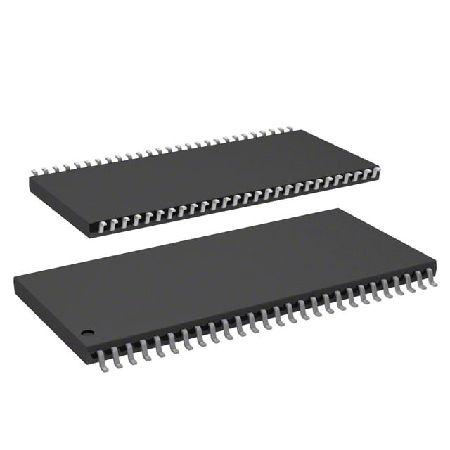
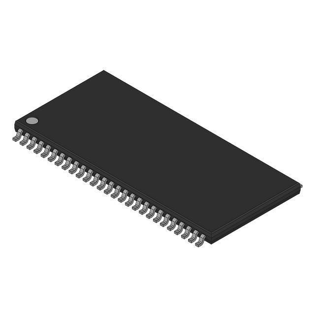
| Device Package | 54-TSOP II | Memory Format | DRAM | Technology | SDRAM | ||
|---|---|---|---|---|---|---|---|
| Memory Size | 64 Mbit | Access Time | 5.4 ns | Grade | Industrial | ||
| Clock Frequency | 143 MHz | Voltage | 3V ~ 3.6V | Memory Type | Volatile | ||
| Operating Temperature | -40°C ~ 85°C (TA) | Write Cycle Time Word Page | N/A | Packaging | 54-TSOP (0.400", 10.16mm Width) | ||
| Mounting Method | Volatile | Memory Interface | Parallel | Memory Organization | 4M x 16 | ||
| Moisture Sensitivity Level | 3 (168 Hours) | RoHS Compliance | ROHS Compliant | REACH Compliance | REACH Unaffected | ||
| Qualification | N/A | ECCN | EAR99 | HTS Code | 8542.32.0002 |
Overview of IS42S16400D-7TLI – IC DRAM 64MBIT PAR 54TSOP II
The IS42S16400D-7TLI is a 64‑Mbit synchronous DRAM organized as 1,048,576 bits × 16 bits × 4 banks (quad‑bank SDRAM) designed for high‑speed, burst‑oriented memory systems. It implements a fully synchronous pipeline architecture with registered inputs and outputs referenced to the rising clock edge, providing predictable timing and bank interleaving for improved random‑access throughput.
This SDRAM targets systems requiring parallel DRAM with programmable burst control, selectable CAS latency, and industrial temperature availability, offering designers flexible timing, power and packaging options for embedded and industrial applications.
Key Features
- Core Organization Quad‑bank architecture organized as 1,048,576 × 16 × 4 banks (64‑Mbit) to enable bank interleaving and reduce precharge latency.
- Performance Supports clock frequencies listed at 166 MHz and 143 MHz with programmable CAS latency of 2 or 3 clocks and random column address capability on every clock cycle for high‑rate burst transfers.
- Burst and Access Control Programmable burst lengths (1, 2, 4, 8, full page) and burst sequences (sequential/interleave), plus burst termination options including burst stop and precharge for flexible data transfer patterns.
- Refresh and Power Modes AUTO REFRESH and SELF REFRESH modes with 4096 refresh cycles every 64 ms, plus power‑down mode to support power management in system designs.
- Interface and Control LVTTL‑compatible inputs/outputs with LDQM/UDQM byte masks, standard SDRAM command signals (CLK, CKE, CS, RAS, CAS, WE) and support for burst read/write and burst read/single write operations.
- Supply and I/O Single 3.3 V supply with specified operating range of 3.0 V to 3.6 V; separate VDDQ/GNDQ for DQ pins to support signal integrity of I/O.
- Package and Temperature Available in a 400‑mil 54‑pin TSOP II (54‑TSOP) package and a 60‑ball fBGA option, with industrial operating temperature range of −40 °C to 85 °C.
Unique Advantages
- Flexible timing configuration: Programmable CAS latency (2, 3) and multiple burst lengths/sequences let designers tune latency and throughput to match system timing requirements.
- Improved random‑access efficiency: Quad‑bank organization and internal bank interleaving hide row precharge time and enable seamless access across banks.
- Power and refresh management: AUTO and SELF REFRESH plus power‑down modes with standard refresh timing (4096 cycles/64 ms) simplify low‑power operation and system reliability.
- Byte‑level control: LDQM and UDQM provide independent upper and lower byte masking for fine‑grained data handling during burst operations.
- Industrial temperature support: Specified operation from −40 °C to 85 °C for deployment in temperature‑sensitive or industrial environments.
- Multiple package options: 54‑TSOP II and 60‑ball fBGA packages accommodate board‑space and assembly preferences.
Why Choose IS42S16400D-7TLI?
The IS42S16400D-7TLI combines a quad‑bank SDRAM architecture with configurable burst behavior and selectable CAS latency to deliver predictable, high‑rate burst transfers and efficient random access in parallel memory systems. Its LVTTL interface, separate DQ power pins, and byte mask signals offer practical control for embedded and industrial designs.
This device is well suited to designs that require a 64‑Mbit SDRAM with industrial temperature capability, flexible timing options, and multiple package choices, providing a stable, configurable memory building block for systems where controlled timing and power management are important.
Request a quote or submit an inquiry to obtain pricing, lead‑time and availability information for IS42S16400D-7TLI.