IS42S16400D-7BLI
| Part Description |
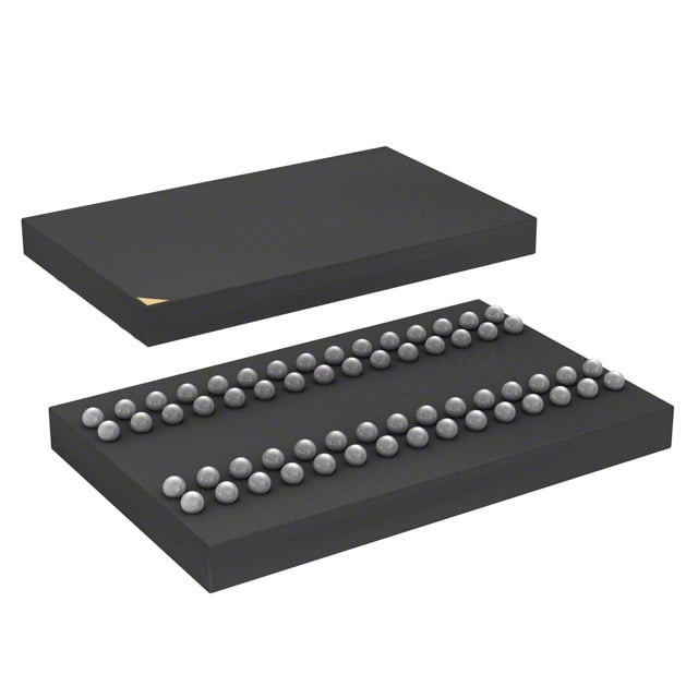
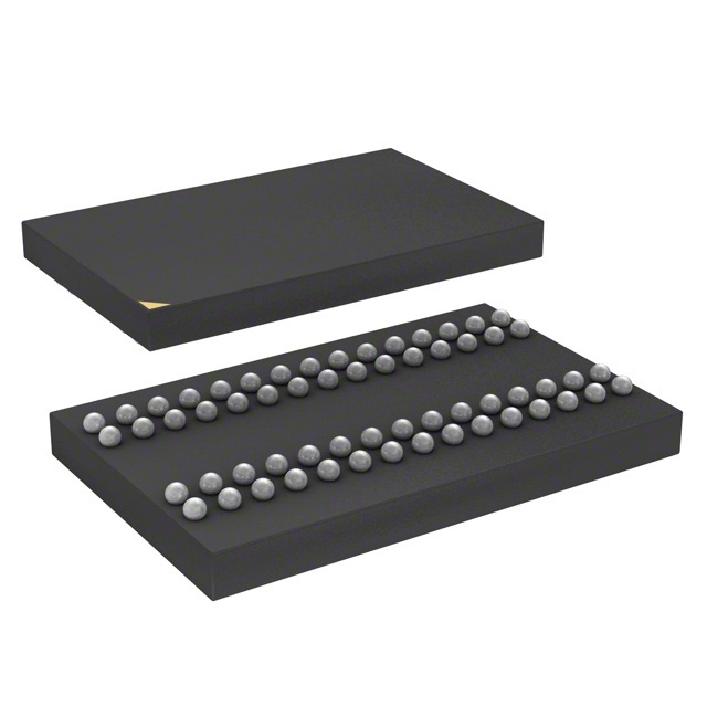
IC DRAM 64MBIT PAR 60MINIBGA |
|---|---|
| Quantity | 1,101 Available (as of June 14, 2026) |

| Product Category | Memory |
|---|---|
| Manufacturer | Integrated Silicon Solution Inc |
| Manufacturing Status | Obsolete |
| Manufacturer Standard Lead Time | Contact Us |
| Datasheet |
Specifications & Environmental
| Device Package | 60-MiniBGA (6.4x10.1) | Memory Format | DRAM | Technology | SDRAM | ||
|---|---|---|---|---|---|---|---|
| Memory Size | 64 Mbit | Access Time | 5.4 ns | Grade | Industrial | ||
| Clock Frequency | 143 MHz | Voltage | 3V ~ 3.6V | Memory Type | Volatile | ||
| Operating Temperature | -40°C ~ 85°C (TA) | Write Cycle Time Word Page | N/A | Packaging | 60-TFBGA | ||
| Mounting Method | Volatile | Memory Interface | Parallel | Memory Organization | 4M x 16 | ||
| Moisture Sensitivity Level | 3 (168 Hours) | RoHS Compliance | ROHS Compliant | REACH Compliance | REACH Unaffected | ||
| Qualification | N/A | ECCN | EAR99 | HTS Code | 8542.32.0002 |
Overview of IS42S16400D-7BLI – IC DRAM 64MBIT PAR 60MINIBGA
The IS42S16400D-7BLI is a 64-Mbit synchronous DRAM organized as 1,048,576 bits × 16 bits × 4 banks. It implements a fully synchronous pipeline architecture with all signals referenced to the rising edge of the clock for high-speed, deterministic memory operations.
Designed for 3.0 V–3.6 V systems (single 3.3 V power supply referenced in the device datasheet), the device supports programmable burst control, selectable CAS latencies, and self-refresh modes, making it suitable for designs that require controlled, burst-oriented parallel memory access across a broad temperature range.
Key Features
- Memory Organization and Capacity — 64 Mbit total, internally configured as 1,048,576 × 16 × 4 banks (4M × 16) to support bank interleaving and improved access concurrency.
- Synchronous SDRAM Core — Fully synchronous operation with all inputs and outputs registered on the positive clock edge and pipeline architecture for high-speed data transfer.
- Clock and Timing — Supports clock frequencies up to 166 MHz and 143 MHz; access time listed at 5.4 ns and programmable CAS latency options of 2 and 3 clocks.
- Burst and Sequencing — Programmable burst lengths (1, 2, 4, 8, full page) and selectable burst sequencing (sequential or interleave) with burst termination via burst stop or precharge commands.
- Refresh and Power Modes — Auto-refresh and self-refresh support with 4,096 refresh cycles every 64 ms and power-down capabilities to manage standby power.
- Interface and I/O — LVTTL-compatible interface with byte control via LDQM and UDQM; parallel memory interface supporting random column address every clock cycle.
- Voltage and Mounting — Specified supply range of 3.0 V–3.6 V; volatile memory mounting type with separate VDD/VDDQ and GND/GNDQ power pins.
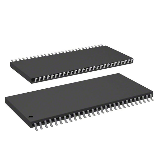
- Package and Temperature — Available in 60-ball mini BGA (60-TFBGA, 6.4 × 10.1 mm) and 54-pin TSOP II packages; industrial temperature availability from −40 °C to 85 °C.
- Byte Masking and Data Control — Byte-level masking supported through LDQM and UDQM signals for controlled write operations on lower and upper byte lanes.
Typical Applications
- Synchronous memory subsystems — For designs requiring deterministic, clocked DRAM behavior and burst-oriented parallel access.
- 3.3 V embedded systems — For systems operating within a 3.0 V–3.6 V supply window that require a parallel SDRAM interface and LVTTL signaling.
- Industrial equipment — Where operation across −40 °C to 85 °C is needed alongside configurable refresh and power modes.
Unique Advantages
- Quad-bank architecture: Internal four-bank organization enables bank interleaving and hides precharge time to improve effective throughput during random and burst access.
- Flexible burst control: Programmable burst lengths and sequences allow tailoring of transfer patterns to match system memory access requirements.
- Selectable CAS latency: CAS latency options (2 and 3) provide timing flexibility to match controller and system timing constraints.
- Robust refresh management: Auto-refresh and self-refresh modes with specified 4,096 refresh cycles per 64 ms ensure data integrity with minimal host intervention.
- Industrial temperature range: Specified operation from −40 °C to 85 °C supports deployment in temperature-challenging environments.
- Compact BGA footprint: 60-ball mini BGA (6.4 × 10.1 mm) enables higher board density for space-constrained designs.
Why Choose IS42S16400D-7BLI?
The IS42S16400D-7BLI provides a compact, synchronous DRAM solution with a 64-Mbit capacity and a quad-bank organization that supports high-performance burst transfers and bank interleaving. With programmable burst lengths, selectable CAS latencies, and a defined operating range of 3.0 V–3.6 V, it fits applications that require precise, clocked memory behavior and configurable timing.
This device is well suited to engineers designing parallel SDRAM interfaces who need predictable timing, refresh control, and operation across an industrial temperature range. Its package options and LVTTL-compatible interface simplify integration into systems that demand compact footprints and standard signaling.
Request a quote or contact sales to discuss availability, lead times, and volume pricing for the IS42S16400D-7BLI.