IS42S16400D-7BL-TR
| Part Description |
IC DRAM 64MBIT PAR 60MINIBGA |
|---|---|
| Quantity | 1,705 Available (as of June 10, 2026) |

| Product Category | Memory |
|---|---|
| Manufacturer | Integrated Silicon Solution Inc |
| Manufacturing Status | Obsolete |
| Manufacturer Standard Lead Time | Contact Us |
| Datasheet |
Specifications & Environmental
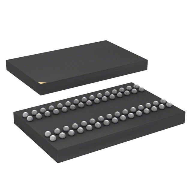
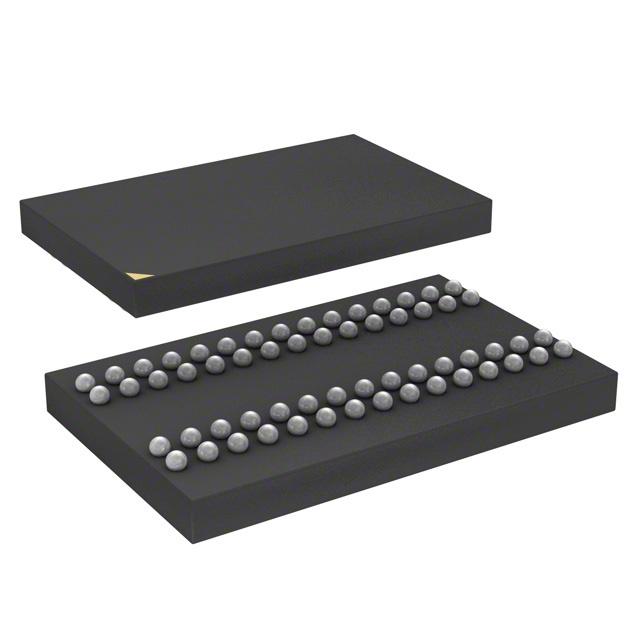
| Device Package | 60-MiniBGA (6.4x10.1) | Memory Format | DRAM | Technology | SDRAM | ||
|---|---|---|---|---|---|---|---|
| Memory Size | 64 Mbit | Access Time | 5.4 ns | Grade | Commercial | ||
| Clock Frequency | 143 MHz | Voltage | 3V ~ 3.6V | Memory Type | Volatile | ||
| Operating Temperature | 0°C ~ 70°C (TA) | Write Cycle Time Word Page | N/A | Packaging | 60-TFBGA | ||
| Mounting Method | Volatile | Memory Interface | Parallel | Memory Organization | 4M x 16 | ||
| Moisture Sensitivity Level | 3 (168 Hours) | RoHS Compliance | ROHS3 Compliant | REACH Compliance | REACH Unaffected | ||
| Qualification | N/A | ECCN | EAR99 | HTS Code | 8542.32.0002 |
Overview of IS42S16400D-7BL-TR – IC DRAM 64MBIT PAR 60MINIBGA
The IS42S16400D-7BL-TR is a 64‑Mbit synchronous DRAM organized as 1,048,576 bits × 16 × 4 banks (64‑Mbit) designed for high‑speed, burst‑oriented memory applications. It implements a fully synchronous pipeline architecture with internal bank interleaving to improve random access throughput in 3.3 V memory systems.
Targeted at systems requiring parallel SDRAM in a compact BGA package, the device offers programmable burst operation, selectable CAS latency, and multiple power‑management modes to balance performance and power consumption.
Key Features
- Memory Architecture – Organized as 1,048,576 × 16 × 4 banks (64‑Mbit) with internal bank interleaving and pipeline architecture for high‑speed burst transfers.
- Synchronous SDRAM Core – Fully synchronous operation with all signals referenced to the rising edge of CLK and LVTTL‑compatible inputs/outputs.
- Clock and Timing – Rated clock frequency listed at 143 MHz with programmable CAS latency of 2 or 3 clocks and an access time of 5.4 ns.
- Burst and Addressing – Programmable burst lengths (1, 2, 4, 8, full page) and selectable burst sequence (sequential or interleave); supports random column address changes every clock cycle.
- Power and Refresh – Single 3.3 V power supply (3.0–3.6 V range), AUTO REFRESH and SELF REFRESH modes, and 4,096 refresh cycles every 64 ms; includes power‑down capability.
- Byte Control and I/O – Byte masking via LDQM and UDQM; VDDQ and GNDQ separate power/ground for DQ pins.
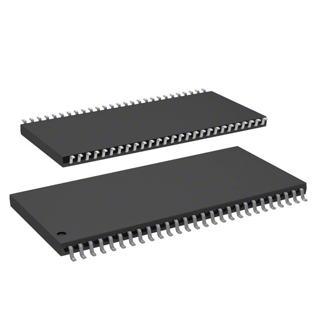
- Package Options – Available in a 60‑ball fBGA / 60‑MiniBGA (6.4 × 10.1 mm) package; also offered in 54‑pin TSOP II format.
- Operating Range – Specified operating ambient temperature range of 0 °C to 70 °C (TA).
Typical Applications
- Embedded Systems – Acts as parallel SDRAM for microcontroller or FPGA‑based designs requiring burst reads/writes and banked access.
- Consumer Electronics – Suitable for devices using 3.3 V SDRAM for frame buffers, temporary data storage, or buffering tasks.
- Networking and Communications Modules – Useful where synchronous burst transfers and internal bank interleaving improve throughput for packet buffering.
Unique Advantages
- Quad‑Bank Interleaving: Internal four‑bank architecture hides row precharge cycles and enables higher effective throughput during random access patterns.
- Flexible Burst Control: Programmable burst lengths and sequence modes let designers optimize for sequential or interleaved access patterns.
- Low‑Level I/O Control: LDQM and UDQM byte masks and separate VDDQ/GNDQ rails provide control over data byte lanes and I/O power domains.
- Power Management Modes: AUTO REFRESH, SELF REFRESH, and power‑down modes help manage refresh and standby power in 3.3 V systems.
- Compact Package: Available in a 60‑ball miniBGA (6.4 × 10.1 mm) for space‑constrained boards while maintaining a parallel SDRAM interface.
Why Choose IS42S16400D-7BL-TR?
The IS42S16400D-7BL-TR delivers a straightforward, fully synchronous 64‑Mbit SDRAM option with quad‑bank architecture, flexible burst operation, and standard 3.3 V interfacing. Its combination of programmable timing (CAS latency), burst control, and power‑management modes makes it suitable for designs that need predictable, burst‑oriented memory behavior in a compact BGA footprint.
This device is well suited for engineers specifying parallel SDRAM in embedded, consumer, or communication products who require clear electrical and timing characteristics and a compact package option for board‑level integration.
For pricing, lead time, or to request a quote for IS42S16400D-7BL-TR, please submit a quote request or contact our sales team for assistance.