IS42S16800D-6T
| Part Description |
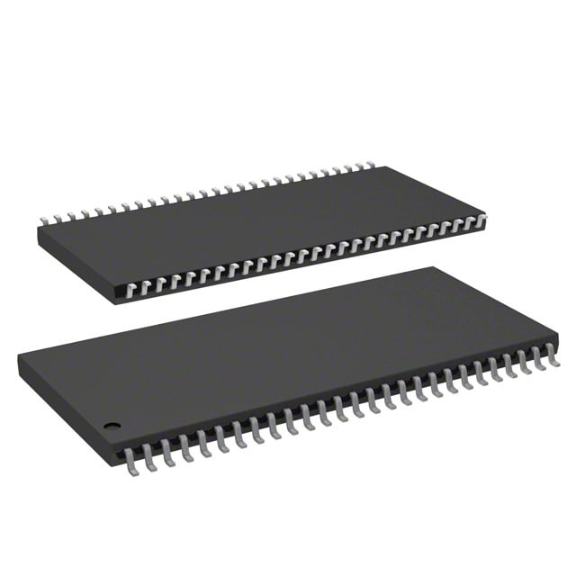
IC DRAM 128MBIT PAR 54TSOP II |
|---|---|
| Quantity | 488 Available (as of June 15, 2026) |

| Product Category | DRAM Memory |
|---|---|
| Manufacturer | Integrated Silicon Solution Inc |
| Manufacturing Status | Obsolete |
| Manufacturer Standard Lead Time | Contact Us |
| Datasheet |
Specifications & Environmental
| Device Package | 54-TSOP II | Memory Format | DRAM | Technology | SDRAM | ||
|---|---|---|---|---|---|---|---|
| Memory Size | 128 Mbit | Access Time | 5.4 ns | Grade | Commercial | ||
| Clock Frequency | 166 MHz | Voltage | 3V ~ 3.6V | Memory Type | Volatile | ||
| Operating Temperature | 0°C ~ 70°C (TA) | Write Cycle Time Word Page | N/A | Packaging | 54-TSOP (0.400", 10.16mm Width) | ||
| Mounting Method | Volatile | Memory Interface | Parallel | Memory Organization | 8M x 16 | ||
| Moisture Sensitivity Level | 3 (168 Hours) | RoHS Compliance | ROHS3 Compliant | REACH Compliance | REACH Unaffected | ||
| Qualification | N/A | ECCN | EAR99 | HTS Code | 8542.32.0002 |
Overview of IS42S16800D-6T – 128‑Mbit Synchronous DRAM, 54‑TSOP II
The IS42S16800D-6T is a 128‑Mbit synchronous DRAM (SDRAM) organized as 8M × 16 with a quad‑bank architecture and pipeline organization for high‑speed data transfer. The device is designed for 3.3V memory systems and implements fully synchronous operation with all signals referenced to the positive clock edge.
Built for systems that require burst‑oriented, low‑latency memory access, the IS42S16800D-6T supports programmable burst lengths and sequences, programmable CAS latency, auto and self refresh modes, and a standard 54‑pin TSOP II package for compact board integration.
Key Features
- Memory Core 128‑Mbit SDRAM organized as 8M × 16 with internal quad‑bank configuration (4 banks) providing 134,217,728 bits of storage.
- Performance Clock frequency up to 166 MHz with access time from clock of 5.4 ns (CAS latency = 3) and CAS latency programmable for 2 or 3 clocks.
- Burst and Sequencing Programmable burst lengths (1, 2, 4, 8, full page) and selectable burst sequence (sequential or interleave) for flexible data transfer patterns.
- Refresh and Power Management Auto Refresh (CBR), Self Refresh with programmable refresh periods, and 4096 refresh cycles every 64 ms; includes power‑down mode for power savings.
- Interface LVTTL‑compatible interface with parallel memory bus and random column address capability every clock cycle for efficient column access.
- Voltage and Supply Designed for VDD = VDDQ = 3.3V (operational supply range listed as 3.0V–3.6V in product specifications).
- Package and Mounting 54‑pin TSOP II (0.400", 10.16 mm width) package, suitable for compact board layouts; supplier device package listed as 54‑TSOP II.
- Operational Range and Availability Operating ambient temperature range of 0°C to 70°C (TA) with industrial temperature availability and lead‑free device availability noted.
- System Features Internal bank interleaving to hide row precharge time, burst termination options (burst stop and precharge), and self‑timed row precharge at burst end when auto precharge is enabled.
Typical Applications
- Synchronous memory subsystems Used as a 128‑Mbit SDRAM component in 3.3V memory systems requiring quad‑bank, burst‑oriented DRAM.
- High‑speed buffering and burst access Suited for designs that require pipeline architecture and programmable burst transfers to support high data throughput.
- Systems requiring low‑latency access Applicable where CAS latency options (2 or 3) and sub‑10 ns access times from clock are required.
Unique Advantages
- Low access latency: Access time from clock as low as 5.4 ns (CAS‑3) provides fast read timing for latency‑sensitive designs.
- Flexible burst control: Multiple burst lengths and sequence modes allow optimization of transfers for sequential or interleaved access patterns.
- Quad‑bank interleaving: Internal bank architecture enables overlapping of precharge and access cycles to improve sustained throughput.
- Comprehensive refresh options: Auto and self refresh modes with programmable periods and standard refresh rate (4096 cycles/64 ms) simplify memory retention management.
- Standard TSOP II packaging: 54‑pin TSOP II package (10.16 mm width) supports compact board integration and established board assembly processes.
- 3.3V system compatibility: Designed for VDD/VDDQ = 3.3V, aligning with common SDRAM memory system supply rails.
Why Choose IS42S16800D-6T?
The IS42S16800D-6T combines a 128‑Mbit SDRAM core with a synchronous, pipeline architecture and quad‑bank organization to deliver predictable, low‑latency burst accesses for 3.3V memory systems. Programmable CAS latency, burst control, and comprehensive refresh and power‑down modes make it a flexible choice for designs that demand configurable timing and power behavior.
This device is well suited to engineers specifying a compact 54‑pin TSOP II SDRAM package with verified timing characteristics (166 MHz clock option, 5.4 ns access time at CAS‑3) and standard LVTTL interface compatibility. Its refresh and bank‑interleave features provide design options to optimize throughput and power management in memory subsystems.
Request a quote or submit a sales inquiry for pricing and availability details for the IS42S16800D-6T.