IS42S16800D-75EBL
| Part Description |
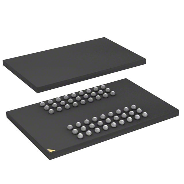
IC DRAM 128MBIT PAR 54MINIBGA |
|---|---|
| Quantity | 770 Available (as of June 14, 2026) |

| Product Category | Memory |
|---|---|
| Manufacturer | Integrated Silicon Solution Inc |
| Manufacturing Status | Obsolete |
| Manufacturer Standard Lead Time | Contact Us |
| Datasheet |
Specifications & Environmental
| Device Package | 54-MiniBGA (8x13) | Memory Format | DRAM | Technology | SDRAM | ||
|---|---|---|---|---|---|---|---|
| Memory Size | 128 Mbit | Access Time | 6.5 ns | Grade | Commercial | ||
| Clock Frequency | 133 MHz | Voltage | 3V ~ 3.6V | Memory Type | Volatile | ||
| Operating Temperature | 0°C ~ 70°C (TA) | Write Cycle Time Word Page | N/A | Packaging | 54-VFBGA | ||
| Mounting Method | Volatile | Memory Interface | Parallel | Memory Organization | 8M x 16 | ||
| Moisture Sensitivity Level | 3 (168 Hours) | RoHS Compliance | ROHS3 Compliant | REACH Compliance | REACH Unaffected | ||
| Qualification | N/A | ECCN | EAR99 | HTS Code | 8542.32.0002 |
Overview of IS42S16800D-75EBL – IC DRAM 128Mbit Parallel 54 MiniBGA
The IS42S16800D-75EBL is a 128 Mbit synchronous DRAM (SDRAM) device organized as 8M × 16 with a quad-bank architecture. It is designed for 3.3V memory systems and provides a fully synchronous, LVTTL-referenced interface for parallel memory implementations.
This device targets systems that require high-speed, burst-oriented memory access with internal bank interleaving, programmable burst behavior and on-chip refresh management.
Key Features
- Memory Core 128 Mbit SDRAM organized as 8M × 16 with a quad-bank internal configuration for concurrent bank operation and efficient row precharge handling.
- Performance Supports clock frequencies of 166, 143 and 133 MHz (device grade options). Typical access time from clock is 6.5 ns for the -75E grade and programmable CAS latency of 2 or 3 clocks.
- Burst and Addressing Programmable burst lengths (1, 2, 4, 8, full page) and selectable burst sequence (Sequential or Interleave) with random column address capability every clock cycle.
- Refresh and Power Modes Auto Refresh (CBR) and Self Refresh with programmable refresh periods; 4096 refresh cycles every 64 ms are supported to maintain data integrity.
- Interface and Logic Levels LVTTL-compatible inputs/outputs and a parallel memory interface for standard system integration.
- Power Nominal 3.3V VDD/VDDQ operation with an operating supply range of 3.0 V to 3.6 V.
- Package and Temperature 54-ball MiniBGA (8 × 13) package in a compact 54-VFBGA form factor; operating temperature range 0°C to 70°C (TA). Lead-free availability noted in the device datasheet.
Typical Applications
- Parallel SDRAM systems — Deploy as a 128 Mbit synchronous DRAM component where a parallel LVTTL SDRAM interface is required.
- Memory expansion modules — Provide organized 8M × 16 memory for designs requiring quad-bank SDRAM capacity in a compact BGA footprint.
- High-speed buffering — Use where burst read/write capability and 133 MHz-class clocking with 6.5 ns access are needed for fast data paths.
Unique Advantages
- Synchronous quad-bank architecture: Internal bank structure and bank interleaving hide row access/precharge times to improve effective throughput.
- Flexible burst control: Programmable burst lengths and sequences enable tailoring of transfer behavior to system access patterns.
- Multiple timing grades: Available clock-frequency grades (166, 143, 133 MHz) and selectable CAS latencies (2 or 3) provide design flexibility for timing and performance trade-offs.
- On-chip refresh management: Auto Refresh and Self Refresh modes with 4096 refresh cycles/64 ms reduce external refresh control complexity.
- Compact BGA package: 54-ball MiniBGA (8×13) reduces PCB area while providing robust soldered connections for dense system designs.
- LVTTL compatibility: Logic-level compatibility simplifies interfacing with standard 3.3V system logic.
Why Choose IS42S16800D-75EBL?
The IS42S16800D-75EBL combines a 128 Mbit SDRAM core with synchronous, LVTTL-referenced operation and a quad-bank architecture to deliver predictable, burst-oriented memory performance. Its supported timing grades and programmable burst/CAS settings make it adaptable to designs that require specific clocking and latency profiles.
This device is well suited for designs that require a compact BGA package, standard 3.3V operation, on-chip refresh features and flexible burst behavior—offering a focused memory solution for engineers optimizing board area and memory timing.
Request a quote or submit a sales inquiry to obtain pricing, availability and lead-time information for the IS42S16800D-75EBL.