IS45S16800B-7TLA1
| Part Description |
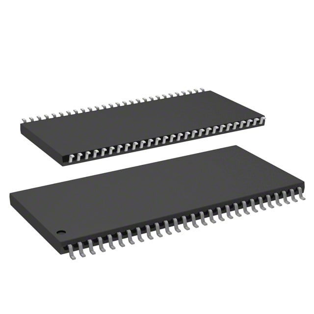
IC DRAM 128MBIT PAR 54TSOP II |
|---|---|
| Quantity | 1,289 Available (as of June 10, 2026) |
| Product Category | Memory |
|---|---|
| Manufacturer | Integrated Silicon Solution Inc |
| Manufacturing Status | Obsolete |
| Manufacturer Standard Lead Time | Contact Us |
| Datasheet |
Specifications & Environmental
| Device Package | 54-TSOP II | Memory Format | DRAM | Technology | SDRAM | ||
|---|---|---|---|---|---|---|---|
| Memory Size | 128 Mbit | Access Time | 5.4 ns | Grade | Industrial | ||
| Clock Frequency | 143 MHz | Voltage | 3V ~ 3.6V | Memory Type | Volatile | ||
| Operating Temperature | -40°C ~ 85°C (TA) | Write Cycle Time Word Page | N/A | Packaging | 54-TSOP (0.400", 10.16mm Width) | ||
| Mounting Method | Volatile | Memory Interface | Parallel | Memory Organization | 8M x 16 | ||
| Moisture Sensitivity Level | 3 (168 Hours) | RoHS Compliance | ROHS3 Compliant | REACH Compliance | REACH Unaffected | ||
| Qualification | N/A | ECCN | EAR99 | HTS Code | 8542.32.0002 |
Overview of IS45S16800B-7TLA1 – IC DRAM 128Mbit SDRAM, 54‑pin TSOP II
The IS45S16800B-7TLA1 is a 128‑Mbit synchronous DRAM organized as 8M × 16 with a parallel SDRAM interface in a 54‑pin TSOP II package. It implements a quad‑bank, fully synchronous architecture with LVTTL signaling and programmable burst modes to support high‑speed, pipelined data transfers.
Designed for board‑level memory expansion and systems requiring predictable timing and extended temperature operation, this device delivers up to 143 MHz clock operation with programmable CAS latency and on‑chip refresh features for continuous data throughput and reliable retention.
Key Features
- Core / Memory Organization 128 Mbit SDRAM organized as 8M × 16 with four internal banks to enable interleaved accesses and hidden precharge operations.
- Performance Supports up to 143 MHz clock frequency (‑7 speed grade) with access time as low as 5.4 ns (CAS latency = 3) and programmable CAS latency of 2 or 3 clocks.
- Burst and Access Modes Programmable burst lengths (1, 2, 4, 8, full page) and burst sequences (sequential/interleave) with burst read/write and burst read/single write capability; burst termination via stop or precharge commands.
- Refresh and Power Management Auto Refresh (CBR) and Self Refresh with programmable refresh periods; 4096 refresh cycles every 64 ms to maintain data integrity.
- Interface and Signaling Fully synchronous interface with all inputs/outputs referenced to the rising clock edge and LVTTL‑compatible I/O.
- Voltage and Supply Operates from 3.0 V to 3.6 V supply range as specified for VDD/VDDQ.
- Package and Temperature 54‑pin TSOP II (0.400", 10.16 mm width) in a compact board‑level package; operating temperature range −40 °C to +85 °C (TA).
Typical Applications
- Parallel SDRAM Memory Subsystems — Use as a 128‑Mbit parallel SDRAM device in designs that require synchronous burst access and LVTTL interface timing.
- High‑speed Buffering and Temporary Storage — Leverage 143 MHz clock operation and programmable burst modes for high‑rate pipeline buffering and data staging.
- Extended‑Temperature Embedded Systems — Suitable for designs requiring operation across −40 °C to +85 °C where consistent memory timing is needed.
- Board‑level Memory Expansion — Compact 54‑pin TSOP II package for integrating 128 Mb of SDRAM in space‑constrained PCBs.
Unique Advantages
- High‑frequency synchronous operation: Supports up to 143 MHz clocking for faster burst transfers and lower access latency (5.4 ns at CL=3).
- Flexible burst control: Programmable burst lengths and sequences simplify interfacing to a variety of controller architectures and access patterns.
- Robust refresh management: Auto and self‑refresh modes with defined refresh cycles (4096/64 ms) reduce external refresh overhead and help maintain data integrity.
- Compact package footprint: 54‑pin TSOP II enables high‑density board implementations while keeping routing and placement predictable.
- Extended operating voltage and temperature: 3.0–3.6 V supply range and −40 °C to +85 °C operating range support stable operation across typical system conditions.
Why Choose IS45S16800B-7TLA1?
The IS45S16800B-7TLA1 offers a practical combination of synchronous, high‑speed SDRAM performance and compact board‑level packaging. Its programmable burst modes, selectable CAS latency, and quad‑bank architecture enable designers to tune memory behavior for throughput‑sensitive, pipeline‑driven applications.
With a defined supply range, LVTTL interface, and extended temperature capability, this 128‑Mbit SDRAM is suited to designs that demand predictable timing, flexible burst control, and reliable on‑chip refresh management over a broad set of operating conditions.
Request a quote or submit a sales inquiry to obtain pricing, availability, or technical support for IS45S16800B-7TLA1.