IS46DR16320C-3DBA2
| Part Description |
IC DRAM 512MBIT PAR 84TWBGA |
|---|---|
| Quantity | 773 Available (as of June 15, 2026) |

| Product Category | Memory |
|---|---|
| Manufacturer | Integrated Silicon Solution Inc |
| Manufacturing Status | Obsolete |
| Manufacturer Standard Lead Time | Contact Us |
| Datasheet |
Specifications & Environmental
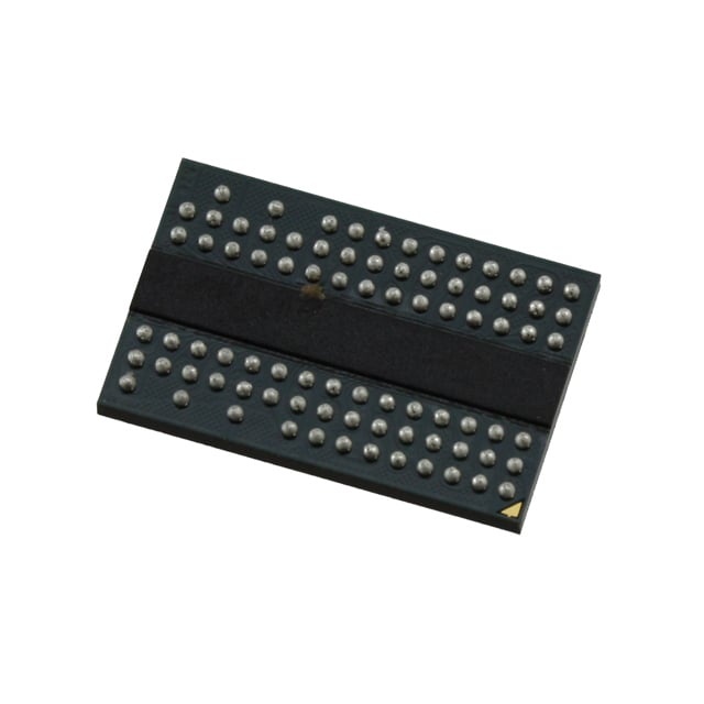
| Device Package | 84-TWBGA (8x12.5) | Memory Format | DRAM | Technology | SDRAM - DDR2 | ||
|---|---|---|---|---|---|---|---|
| Memory Size | 512 Mbit | Access Time | 450 ps | Grade | Automotive | ||
| Clock Frequency | 333 MHz | Voltage | 1.7V ~ 1.9V | Memory Type | Volatile | ||
| Operating Temperature | -40°C ~ 105°C (TA) | Write Cycle Time Word Page | 15 ns | Packaging | 84-TFBGA | ||
| Mounting Method | Volatile | Memory Interface | Parallel | Memory Organization | 32M x 16 | ||
| Moisture Sensitivity Level | 3 (168 Hours) | RoHS Compliance | ROHS Compliant | REACH Compliance | REACH Unaffected | ||
| Qualification | N/A | ECCN | OBSOLETE | HTS Code | N/A |
Overview of IS46DR16320C-3DBA2 – IC DRAM 512MBIT PAR 84TWBGA
The IS46DR16320C-3DBA2 is a 512 Mbit DDR2 SDRAM organized as 32M × 16 with a parallel memory interface. It implements a double-data-rate architecture with a 4-bit prefetch to deliver two data transfers per clock cycle for high-speed memory operation.
Designed for system-level memory subsystems, the device targets applications that require compact, low-voltage DDR2 memory with programmable timing, on-die termination, and differential data strobe support.
Key Features
- Memory Core 512 Mbit DDR2 SDRAM organized as 32M × 16 with four internal banks and a 4-bit prefetch architecture.
- Double-Data-Rate Interface Two data transfers per clock cycle with differential data strobe (DQS / DQS̅) and on-chip DLL to align DQ and DQS transitions with CK.
- Programmable Timing Programmable CAS latency (CL = 3, 4, 5, 6) plus posted CAS and programmable additive latency (AL = 0–5); write latency = read latency − 1 tCK.
- Burst and Drive Options Programmable burst lengths of 4 or 8 and adjustable data-output drive strength (full and reduced strength options).
- Signal Integrity On-die termination (ODT) and JEDEC-standard 1.8V I/O (SSTL_18-compatible) to simplify board-level termination and signal integrity.
- Performance and Timing Key timing examples from the device family include tCK options and cycle times (examples: 3.0 ns and 2.5 ns class timings shown in datasheet); specified access time is 450 ps.
- Power Low-voltage operation with VDD / VDDQ supply range of 1.7 V to 1.9 V (VDD = 1.8 V ±0.1 V per datasheet).
- Package and Temperature 84-ball WBGA package (8 mm × 12.5 mm) and a wide operating ambient range shown as −40°C to 105°C (TA) in product specifications.
Typical Applications
- Embedded memory subsystems Use as a compact DDR2 memory component where 512 Mbit density and parallel DDR2 interface are required.
- High-speed buffering Suitable for system designs that need double-data-rate transfers and programmable burst lengths for burst-oriented data movement.
- Industrial systems Applicable in environments requiring wide ambient operating range (specified to −40°C to 105°C TA) and robust low-voltage DRAM operation.
Unique Advantages
- Low-voltage DDR2 operation: Operates from 1.7 V to 1.9 V with JEDEC-standard 1.8 V I/O, enabling lower-power system designs that adhere to SSTL_18 signaling.
- Flexible timing control: Programmable CAS latencies, additive latencies, and burst lengths let designers optimize latency and throughput trade-offs for specific workloads.
- Signal integrity features: On-die termination and adjustable drive strength reduce external termination complexity and help maintain signal quality at high data rates.
- Compact WBGA package: 84-ball WBGA (8 mm × 12.5 mm) provides a space-efficient footprint for dense system layouts.
- Wide operating temperature: Specified ambient range down to −40°C supports use in temperature-challenging installations.
Why Choose IC DRAM 512MBIT PAR 84TWBGA?
The IS46DR16320C-3DBA2 positions itself as a practical DDR2 memory building block for designs that require a 512 Mbit density, low-voltage 1.8 V operation, and flexible timing control. Its DDR2 double-data-rate architecture, on-chip DLL, differential DQS, and ODT provide the signal and timing features needed for reliable high-speed transfers in compact footprints.
This device is well suited for engineers designing embedded memory subsystems and high-speed buffers who need a verifiable, specification-driven DRAM element with programmable latency and drive options. The combination of package, voltage range, and operating temperature supports integration into a variety of industrial and system-level applications.
Request a quote or submit an inquiry to receive pricing and availability information for the IS46DR16320C-3DBA2 and to discuss how it fits your design requirements.