MT48LC64M8A2TG-75:C TR
| Part Description |
IC DRAM 512MBIT PAR 54TSOP II |
|---|---|
| Quantity | 469 Available (as of June 14, 2026) |
| Product Category | Memory |
|---|---|
| Manufacturer | Micron Technology Inc. |
| Manufacturing Status | Obsolete |
| Manufacturer Standard Lead Time | Contact Us |
| Datasheet |
Specifications & Environmental
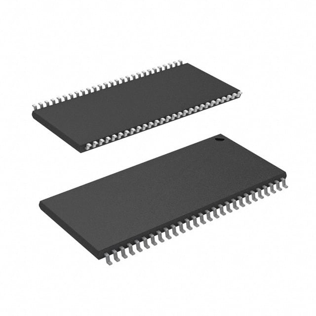
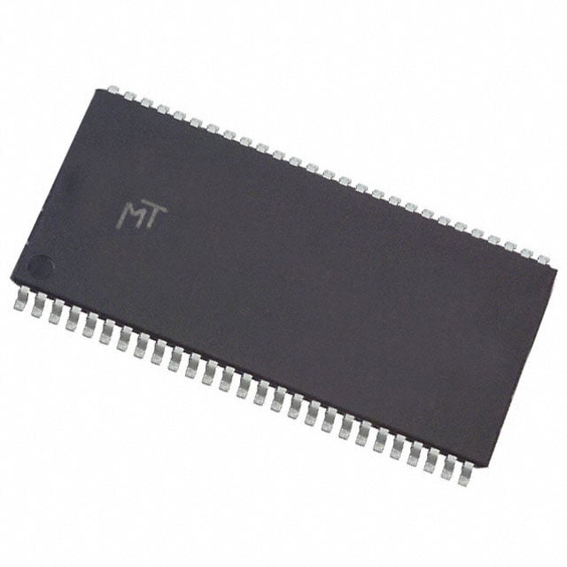
| Device Package | 54-TSOP II | Memory Format | DRAM | Technology | SDRAM | ||
|---|---|---|---|---|---|---|---|
| Memory Size | 512 Mbit | Access Time | 5.4 ns | Grade | Commercial | ||
| Clock Frequency | 133 MHz | Voltage | 3V ~ 3.6V | Memory Type | Volatile | ||
| Operating Temperature | 0°C ~ 70°C (TA) | Write Cycle Time Word Page | 15 ns | Packaging | 54-TSOP (0.400", 10.16mm Width) | ||
| Mounting Method | Volatile | Memory Interface | Parallel | Memory Organization | 64M x 8 | ||
| Moisture Sensitivity Level | 4 (72 Hours) | RoHS Compliance | RoHS non-compliant | REACH Compliance | REACH Unaffected | ||
| Qualification | N/A | ECCN | EAR99 | HTS Code | 8542.32.0024 |
Overview of MT48LC64M8A2TG-75:C TR – IC DRAM 512MBIT PAR 54TSOP II
The MT48LC64M8A2TG-75:C TR is a 512 Mbit synchronous DRAM organized as 64M × 8 with a parallel SDRAM interface in a 54‑pin TSOP II (0.400", 10.16 mm width) package. It implements SDR SDRAM architecture with fully synchronous, positive-edge clocked signaling, internal pipelined operation and internal banks for optimized row access and precharge management.
Designed for systems requiring a 512 Mbit parallel SDRAM device, the device offers PC100 and PC133 compliance, programmable burst lengths, and standard single‑supply operation, making it suitable for board-level memory implementations that need a 54‑TSOP footprint and commercial temperature range operation.
Key Features
- Memory Architecture: 64M × 8 organization providing 512 Mbit density with 4 internal banks to improve access concurrency.
- SDR SDRAM Core: Fully synchronous SDRAM with all signals registered on the positive edge of the system clock; internal pipelined operation allows column address changes every clock cycle.
- Performance / Timing: PC100- and PC133‑compliant operation with a maximum clock frequency of 133 MHz and an access time of 5.4 ns (CL = 3 at -75 speed grade).
- Programmable Burst and Refresh: Supports programmable burst lengths (1, 2, 4, 8, or full page), auto precharge, auto refresh, and self refresh modes with 8192‑cycle refresh (64 ms interval).
- Interface Compatibility: Parallel memory interface with LVTTL‑compatible inputs and outputs for standard SDRAM signalling.
- Power Supply: Single 3.3 V supply (3.0 V to 3.6 V specified); write cycle time (word/page) 15 ns.
- Package and Mounting: 54‑pin TSOP II (400 mil) plastic package (54‑TSOP II, TG marking) suitable for PC board mounting.
- Operating Range: Commercial temperature operation 0°C to +70°C (TA) as specified for the standard device.
Typical Applications
- PC100/PC133 memory subsystems: Use in systems requiring PC100 or PC133‑compliant SDRAM devices for synchronous parallel memory implementations.
- Board-level memory expansion: 512 Mbit density in a 54‑TSOP II package for designs needing higher DRAM capacity in a compact footprint.
- Legacy parallel SDRAM designs: Direct replacement or integration for systems using parallel SDRAM interfaces with LVTTL‑compatible signaling and single 3.3 V supply.
Unique Advantages
- PC100/PC133 Compliance: Conforms to common PC100 and PC133 timing grades, enabling integration into established synchronous memory subsystems.
- Pipelined, Banked Architecture: Internal pipelining and multiple banks reduce effective row‑access latency by allowing column changes every clock cycle.
- Flexible Burst Control: Programmable burst lengths (1, 2, 4, 8, full page) provide adaptable data-transfer modes for varied system requirements.
- Standard 3.3 V Supply: Single 3.0 V to 3.6 V operating range simplifies power design for systems using 3.3 V rails.
- Compact TSOP II Package: 54‑pin TSOP II (400 mil) package delivers 512 Mbit density in a board‑level friendly footprint.
- Refresh and Low‑Power Modes: Supports auto refresh and self refresh to meet dynamic refresh requirements and reduce system management overhead.
Why Choose MT48LC64M8A2TG-75:C TR?
The MT48LC64M8A2TG-75:C TR combines a 512 Mbit SDRAM density with a fully synchronous, pipelined SDRAM architecture and PC100/PC133 timing compatibility, delivering a straightforward memory solution for parallel SDRAM systems that require a 54‑pin TSOP II footprint and standard 3.3 V operation. Its programmable burst lengths, internal banking and refresh modes support efficient data transfers and simplified memory management at the board level.
This part is well suited to designs that need a commercial‑grade SDRAM device with defined timing (5.4 ns access at CL = 3, 133 MHz) and a compact package. It provides long‑term design stability through standard SDRAM features and vendor‑specified electrical and timing parameters.
Request a quote or submit an inquiry to obtain pricing and availability information for the MT48LC64M8A2TG-75:C TR.